webinar banner AI 2026 v2

How HCL VersionVault Works – Directory Versioning

How HCL VersionVault Works – Directory Versioning
by Mike Gianfagna on 09-10-2020 at 10:00 am

Pieter Gosselink Senior Technical Support Engineer HCL Technologies

Last month, I discussed a webinar about HCL VersionVault – HCL VersionVault Delivers Version Control and More. This webinar introduced the HCL VersionVault product. This post will discuss a new video entitled “How HCL VersionVault Works – Directory Versioning.”

To recap, VersionVault delivers a lot of capabilities to the software development process. These include:

  • Version control software
  • Enterprise class (unlimited scalability and the ability to handle very complex structures)
  • Easy to use with a built-in configuration management process
  • Good for regulated industries thanks to built-in authoritative auditing capabilities
  • Reduces time for embedded system development
  • Can synchronize design among a globally disparate development team

Also discussed during the webinar was the virtual file system and the benefits that technology delivered. Recently, HCL has released a new video that digs into aspects of the file system inside VersionVault. While this kind of detail isn’t for everyone, I find it refreshing that HCL is providing this level of insight into how their product works.

Successful deployment of any enterprise tool requires a broad spectrum of participation and stakeholders. An easy to use product that is supported by good training and documentation is a necessary condition for success. If the product solves a well-known problem in an efficient way (from the user’s perspective) that helps a lot with adoption. For all this to work, there needs to be a broader infrastructure and stakeholder list, however.

Typically, power users will lead the way to adoption and others will follow. These users are supported by the development team and typically require insights into how the tool works that go well beyond what an average user would care about. The recent video on how directory versioning works in VersionVault provides the kind of insights these users will need. I was encouraged to see HCL deliver these details, I’m sure it will help with the adoption process.

The video isn’t done in a typical webinar format. It is presented by Pieter Gosselink, senior technical support engineer at HCL Technologies. Peter is behind a clear glass. He uses this surface as a white board to illustrate his points. It’s a clever way to deliver the content since you get to see both the speaker and the annotation on the full screen. It does require Peter to write backwards, which is impressive.

Peter’s video is short (~ 5 minutes), so if you have interest in learning about the inner workings of VersionVault I encourage you to watch it. Here are some of the basics to whet your appetite:

  • The VersionVault file system is based on a combination of directories and file elements organized in a tree-like structure
  • Like file elements, directories can have versions
  • The first version of a directory is empty
  • It should be noted that files get their names from data in the directory elements. This is how Unix works we well
  • When a directory version is populated, each file will be represented by a record number and file name (the record number is part of the file element as well)

Peter goes on to explain how versioning of directories is implemented and how those structures track the files associated with each directory version, ensuring all data is accounted for under all circumstances.

You can watch the video, “HCL VersionVault Works – Directory Versioning” here. If you’d like to watch the webinar on the product, you can access the replay of Introducing HCL VersionVault here. You can also learn more about HCL VersionVault here.

About HCL Technologies

HCL Technologies (HCL) empowers global enterprises with technology for the next decade today. HCL’s Mode 1-2-3 strategy through its deep-domain industry expertise, customer-centricity and entrepreneurial culture of ideapreneurship™ enables businesses transform into next-gen enterprises.

HCL offers its services and products through three business units – IT and Business Services (ITBS), Engineering and R&D Services (ERS) and Products & Platforms (P&P). ITBS enables global enterprises to transform their businesses through offerings in areas of Applications, Infrastructure, Digital Process Operations and next generational digital transformation solutions. ERS offers engineering services and solutions in all aspects of product development and platform engineering while under P&P, HCL provides modernized software products to global clients for their technology and industry specific requirements. Through its cutting-edge co-innovation labs, global delivery capabilities and broad global network, HCL delivers holistic services in various industry verticals, categorized under Financial Services, Manufacturing, Technology & Services, Telecom & Media, Retail & CPG, Life Sciences & Healthcare and Public Services.

As a leading global technology company, HCL takes pride in its diversity, social responsibility, sustainability and education initiatives. As of 12 months ended June 30, 2020, HCL has a consolidated revenue of US $ 9.93 billion and its 150,287 ideapreneurs operate out of 49 countries. For more information, visit https://www.hcltech.com/


Emulation as a Service Benefits New AI Chip

Emulation as a Service Benefits New AI Chip
by Bernard Murphy on 09-10-2020 at 6:00 am

Emulation as a Service

It’s no secret that innovation in AI chip architectures is on a tear. When you put together the spatial complexity of highly parallelized algorithms with the need to localize memory accesses on-chip to the greatest extent possible, we’re seeing a proliferation of all kinds of domain-specific architectures. Which in the normal cycle of these things inevitably leads to wondering if there might be a good general-purpose architecture for AI chips. One recent entry in this field is from Simple Machines, based in San Jose. They have a novel approach they call Composable Computing, in which they build on four fundamental behaviors: data gathering, computational dataflow, synchronization between algorithm stages, and control. Using this platform, they illustrate how they can reconfigure on-the-fly to implement multiple different types of accelerator. To do that, the needed help from Emulation as a Service (EaaS).

Early software prove-out through EaaS

The tricky part is the software. To take advantage of that composability and specialization in behaviors a compiler needs to manage computation placement, data routing, event timing, resource utilization and other goals. This is not a regular compiler and must be tested very carefully. Compounding the problem, workloads for AI engines are huge. So how are you going to test, debug and refine that software while the hardware is still in development?

The normal answer would be an FPGA prototype. Which would work for a small inference engine. But these big general-purpose engines are designed for training as well as inference. They barely fit in an SoC reticle, much less in a single FPGA. And custom FPGA boards come with their own problems. So Simple Machines turned to emulation, with Mentor.

The emulation challenge for startups

Simple Machines is a young company, still on their Series A round and still proving themselves to early stage customers. I’m guessing that they are talking to strategic investors who might want to participate in a Series B round. To raise that level of interest, Simple Machines will need to show a proof of concept to those investors, perhaps early silicon or an emulation prototype. But emulators are expensive. How could Mentor help?

Through Emulation as a Service is how. The ‘as a Service’ concept has taken off widely for organizations that doesn’t have the constant heavy workloads to justify purchasing hardware and software. Emulation needs in a startup are a good example of a cyclic need. Simple Machines can buy access in blocks rather than buying the emulator.

The EaaS flow

John Anderson, Verification Consulting Manager at Mentor told me how this works. Mentor establishes a secure chamber (a virtual Linux host) loaded with Mentor software for emulation and debugging. They also establish an encrypted Mentor Secure Transport (MST) channel for a customer to support secure transfer of data between their site and that chamber. That customer also gets remote desktop software to allow VPN-like access to their own chamber.

As needed Simple Machines were able to upload their design and software to the chamber. The Mentor’s EaaS team provided expert consulting to optimize the cost- and time-efficiency advantages of the Veloce emulation hardware technology. Simple Machines could then compile code, launch jobs, debug and edit designs in the remote chamber via their desktop interface. Once they were done, they could pull results back to their own machines via MST.

Performance and power modeling

One more noteworthy point. Simple Machines were using EaaS not only to model performance but also to model power consumption to assess key power metrics in this pre-silicon design. Modeling the most important aspects of their prototype in preparation for discussions with those strategic investors.

You can read the press release HERE.

Also Read:

WEBINAR: Addressing Verification Challenges in the Development of Optimized SRAM Solutions with surecore and Mentor Solido

Creating Analog PLL IP for TSMC 5nm and 3nm

Getting Physical to Improve Test – White Paper


Analog Bits at TSMC OIP – A Complete On-Die Clock Subsystem for PCIe Gen 5

Analog Bits at TSMC OIP – A Complete On-Die Clock Subsystem for PCIe Gen 5
by Mike Gianfagna on 09-09-2020 at 10:00 am

Design Integration of Complete On die Clock Subsystem for PCIe Gen 5

This is another installment covering TSMC’s very popular Open Innovation Platform event (OIP), held on August 25. This event presents a diverse and high-impact series of presentations describing how TSMC’s vast ecosystem collaborates with each other and with TSMC.  The talk covered here focuses on a complete on-die clock subsystem for PCIe Gen 5. Alan Rogers, president and CTO of Analog Bits, provided detail and motivation regarding the need for on-chip clock support to facilitate high-performance communication subsystems.

A memorable quote from Alan was “we will discuss how to synchronize the serial data interfaces which can move tens of billions of bits of data each and every second on and off a chip through a pair of wires.”

Alan began with a historical perspective on data communications. He pointed out that historically a SerDes would be supplied with a discrete clock chip, provided on the PCB. This worked fine when the SerDes had a limited number of high-end lanes that were not cost constrained. He went on to explain that today, there are a very high number of SerDes lanes and clock synchronization off-chip becomes very difficult to achieve. Performance demands are simply inconsistent with inter-chip transmission of remote clock sources. The system constraints in terms of dollars, power or pin count preclude a non-integrated solution.

With this motivation, Alan explored some of the on-chip options offered by Analog Bits. He provided an example to illustrate the scope and flexibility that can be achieved. The example, shown on the right, provides autonomous clocking of multiple SerDes protocols integrated on TSMC 16FFC technology with a combined clock unit. This example illustrates multiple rows of Analog Bits SerDes and seven coils of independent LC PLLs, each capable of driving a different frequency with a different spectral modulation to any of tens to hundreds of SerDes.

Central to a high frequency clock generator is a high performance PLL. Alan provided several examples of the types of PLLs supported by Analog Bits. These technologies provide a range of jitter, speed, power and area for various applications. Some, such as the LC oscillator design, work best only at high frequencies. The figure below summarizes the various options.

Alan then illustrated several examples of Analog Bits clocking solutions for various applications in several technologies. These included:

  • A ring-based chip-to-chip clock generator in TSMC N7
  • A PLL for cost-sensitive applications supporting PCI Gen 2/3 data rates
  • A PCIe Gen 5 reference clock in TSMC N7/6

Silicon measurements of spread spectrum PLLs in TSMC 16FFC were presented. The data showed very good correlation to simulation results. Data for best-case conditions (FF wafers, high BW, high VCO amp) and worst-case conditions (SS wafers, low BW, low VCO amp) was presented. Closed-loop transient noise vs. silicon data was also reviewed.

Regarding collaboration with TSMC, Alan described an N6 test chip that taped out in June 2020. On board was a large complement of Analog Bits IP, including:

  • Ring OSC PLL
  • LC PLL
  • Bandgap
  • OSC pads
  • RC oscillator
  • TX/RX IO’s

Alan described the customizable architectures available from Analog Bits to clock numerous protocols, including:

  • 16FFC: PCIe 3/4, SATA, SAS3/4, XFI, 10—KR
  • N7/N6: PCIe 3/4/5 and can be expanded to other protocols
  • N5: Available soon for PCIe 4/5, SATA, Ethernet

Clearly, Analog Bits provides a complete on-die clock subsystem for PCIe Gen 5 and beyond. Alan concluded by stating that Analog Bits has been a long-term partner of TSMC, providing a wide range of popular mixed signal IP for many applications. You can learn more at https://www.analogbits.com.

Also Read:

Cerebras and Analog Bits at TSMC OIP – Collaboration on the Largest and Most Powerful AI Chip in the World

AI processing requirements reveal weaknesses in current methods

7nm SERDES Design and Qualification Challenges!


Highlights of the TSMC Technology Symposium – Part 3

Highlights of the TSMC Technology Symposium – Part 3
by Tom Dillinger on 09-09-2020 at 8:00 am

CoWoS features

Recently, TSMC held their 26th annual Technology Symposium, which was conducted virtually for the first time.  This article is the last of three that attempts to summarize the highlights of the presentations.  This article focuses on the technology design enablement roadmap, as described by Cliff Hou, SVP, R&D.

Key Takeaways

  • Design enablement is available for N7, N6, N5, and N3, both EDA reference flows and Foundation IP.
  • N3 “specialty” IP is in development, in collaboration with the IP Partners.
  • Automotive (AEC-Q100) Grade 1 qualification is progressing for N7, offering an attractive PPA migration from N16 (available 4Q20).
  • EDA tool support is available for leading 2.5D/3D package technologies:  SoIC, InFO, CoWoS.  New EDA flow support required for (>1X reticle size) packages will be available 4Q20 (e.g., package warpage analysis).

Introduction

It is no secret that a major factor in TSMC’s foundry success has been the investment in the design enablement ecosystem, which spans the collaboration between TSMC and:

EDA partners

  • enhancing tool algorithms for new process node requirements, from place-and-route to physical design layout verification
  • collaborating with TSMC on implementation of trailblazing designs, from process bring-up memory array testsites to advanced Arm cores
  • preparing an integrated (and qualified) “reference flow” for a new process node

IP providers

  • developing critical IP functionality in a new node to complement TSMC’s Foundation IP
  • qualifying test silicon in the new node for the various TSMC platforms – IoT, mobile, HPC, and (the most demanding) automotive

Design Center Alliance (DCA) service providers

  • offering a range of front-end design resources, back-end implementation skills, custom design support, and DFT services

Value Chain Aggregator (VCA) providers

  • offering a broad range of support, throughout the IC “value chain”, extending all the way from product architecture definition to final wafer assembly/test/qualification services

and, the most recent addition to the Open Innovation Platform (OIP) ecosystem,

Cloud Alliance partners

  • collaborates with TSMC and EDA partners to provide a secure, scalable cloud compute environment for some (i.e., burst demand) or all of the IC design flow

The heart of the Open Innovation Platform is the TSMC Design Enablement (DE) organization.  Cliff provided an update on the enablement status for the upcoming advanced process nodes and packaging technologies, across the various design platforms.

Tool Certification

It should be noted that EDA tool certification at a new node is far more complex than simply running a set of SPICE circuit simulations and updating the runsets used for DRC/LVS/ERC physical verification.  Each node transition commonly introduces new, complex layout design rules, often requiring significant algorithm development by the EDA partner to provide the functionality and language commands needed to code the runset.  Multi-patterning, forbidden pitches, run-length dependent rules, line cut rules, and specific fill requirements across multiple mask levels all have been introduced at recent nodes.  For block composition flows at successive nodes, each cell library may have rules that define new constraints on cell placement, pin access routing, and power distribution/gating.  Reaching tool/flow production certification is no mean feat.

Additionally, new process nodes (and their application markets) may necessitate the introduction of completely new flows:

  • an “aging flow” that integrated the effects of NBTI, PBTI, and HCI into a measure of performance degradation over time, using new device aging models
  • a local heating flow that reflects how the unique thermal dissipation paths in FinFET-based designs impact chip failure mechanisms (especially electromigration)

N7/N6/N5/N3

  • full EDA tool certification, for both custom IP design and cell-based block composition, for all nodes (N5:  v0.9 PDK;  N3:  v0.1 PDK)
  • EDA “utility” certification (e.g., fill algorithms)

(Cliff’s certification charts focus on tool offerings from the major EDA Partners.)

N6 is a variant of N7, offering a yield improvement (fewer mask layers) and the ability to achieve a logic block density improvement using an optimized N6 high-density cell library.

  • N7 automotive platform flows and IP ready (AEC-Q100 Grade 1)
  • N5 automotive platform in 2022 (Grade 1)

Note that there are two common reliability qualification designations for the AEC-Q100 automotive platform, both based on zero fails after 1K hours HTOL stress test on sampled lots, plus HAST and temperature cycling endurance tests:   Grade 1:  -40C to 125C;  Grade 0:  -40C to 150C  (for “under the hood” applications).

When describing the (Grade 1) qualification activity for N7 and N5, Cliff highlighted some of the additional design enablement considerations for the automotive platform:

  • a “low DPPM” Design Rule Manual and DRC runset
  • aging model qualified for the automotive part lifetime and operating temperature
  • automotive platform-specific EM rules
  • automotive platform-specific latchup and ESD design rules
  • soft error upset analysis

Since the automotive “defect parts per million” shipped criterion is stringent, a specific set of DRC rules at the node is employed.

The demand for high-throughput, low power computation in the vehicles of the future is great , and must also meet the AEC-Q100 qualification criteria (Grade 1).  The TSMC design enablement team is extending the technology definition, design rules, models, and Foundation IP evaluation to provide this support at advanced process nodes.

N12e

At the Symposium, TSMC introduced a new ultra low power N12FFC+ variant, denoted as N12e.  This process is specifically designed for IoT (and AIoT, or AI at the edge) applications, offering a transition from N22ULL (planar) to N12e (FinFET).

  • N12e EDA tools certified (major new features added, listed below)

The design enablement for N12e is faced with the challenges of:

  • analyzing and modeling layout dependent effects (LDE), where device impacts are magnified at low VDD
  • developing SPICE models valid for VDD=0.4V
  • providing statistical device model support valid for low VDD operation
  • providing cell characterization, delay calculation, and static timing analysis support valid for low VDD operation;  specific focus is required for flip-flop setup/hold measures at low VDD

(At low supply voltage, the cell delay arc statistical variation is decidedly non-Gaussian, due to the “near Vt” operation.)

Advanced Packaging:  SoIC, InFO, CoWoS  (3D Fabric) 

With the rapid growth of 2.5D and 3D packaging options, the TSMC Design Enablement team has expanded their scope to include the appropriate physical verification and electrical/thermal analysis EDA flow support:

  • redistribution Layer (RDL) routing and through via routing rules (through CoWoS silicon interposer or InFO wafer compound)
  • routed interconnect impedance matching and shielding requirement (e.g., on a CoWoS interposer, to support wide bus width connectivity to HBM stacks)
  • die-to-die bond rules (SoIC)
  • LVS verification throughout the 2.5D/3D package connectivity
  • RC and RLC parasitic extraction for a complex package geometry – especially, inter-die coupling capacitance for SoIC
  • IR and EM analysis of the power distribution network throughout the package assembly
  • signal integrity analysis
  • thermal analysis – especially, through 3D stacked die
  • ESD analysis

EDA tools are ready for SoIC (3D), InFO and CoWoS (both 2.5D), with the following exceptions, as new flows need to be certified:

  • large (>>1X max reticle size) multi-die floorplan package “warpage analysis”  (available for InFO and CoWoS in 4Q20)
  • static timing analysis for stacked die in an SoIC, with temperature/voltage distribution and “multi-corner” process variation between die (available 4Q20)


The TSMC Design Enablement team continues to provide EDA tool and reference flow support for the challenges introduced by advanced process nodes, ranging from new aging models to timing/electrical analysis at low VDD operation.  The 2.5D and 3D package technology offerings require a close collaboration between TSMC and EDA developers to address new requirements – e.g., unique package interconnect/via design rules, stacked die timing analysis.

As mentioned above, TSMC’s focus on design enablement distinguishes their process and package technology offerings.

For more information on the TSMC Design Enablement support for the OIP Partners and platforms, please follow these links – OIP and Technology Platforms.

-chipguy

Highlights of the TSMC Technology Symposium – Part 1

Highlights of the TSMC Technology Symposium – Part 2


Blue Cheetah Technology Catalyzes Chiplet Ecosystem

Blue Cheetah Technology Catalyzes Chiplet Ecosystem
by Tom Simon on 09-09-2020 at 6:00 am

Blue Cheetah Ecosystem

There are many reasons today for dividing up large monolithic SoCs into chiplets that are connected together inside a single package. Let’s look at just some of these reasons. Many SoCs share a common processing core with application specific interfaces and specialized processing engines. Using chiplets would mean that it is easier to reuse the main processing core and ancillary blocks to easily build special purpose IC’s for various markets. Mixing analog and digital functions on a single die can be difficult, especially at more advanced nodes. It would be more cost effective and simpler to build separate analog chiplets and interface them with digital die. Yield is also an issue. The larger a die is the more likely it is that there can be a defect or fabrication failure. This is especially painful when the entire chip has to be rejected. A failed chiplet can be discarded easily without adversely affecting the other parts of a large chiplet based IC design. The list of advantages goes on, but I think you get the idea.

Of course, chiplet based designs introduce new requirements and have some drawbacks. However, it has been pointed out that Gordon Moore saw the potential advantages of this approach back in 1964 when he said, “It may prove to be more economical to build large systems out of smaller functions, which are separately packaged and interconnected.” I recently saw this quote in a presentation from DAC by Intel, CHIPS Alliance and Blue Cheetah. The first issue that needs to be dealt with to make chiplets effective and practical is providing a method for interfacing them to each other.

To address this need, CHIPS Alliance developed the Advanced Interface Bus (AIB), which offers a standardized high bandwidth interface between chiplets. It uses wide parallel connections with dense microbump arrays. It can work at modest clock rates and can transfer massive amounts of data. The topic of AIB and its features is a whole other discussion from the DAC presentation. What Intel, Blue Cheetah and the CHIPS Alliance wanted to talk about is how to rapidly implement the analog AIB PHY for each technology node used in all the chiplets found in a design.

So-to-speak, this is where the rubber meets the road. When dividing up monolithic SoC’s into chiplets each one will need to have an AIB PHY implemented as an analog block – which is traditionally a difficult and time-consuming specialized design task. This is where Blue Cheetah comes in. They have been extending the BAG Framework, initially developed at UC Berkeley, to create generators for producing fully automated analog designs, from schematics and layouts to test benches, LEFs, LIBs, and behavioral models. While not all their generators are open source, the AIB PHY is freely available on GitHub. The BAG framework is also open source, making this a revolutionary proposition.

We are accustomed to open source software and development libraries and even tools. However, in the world of hardware design, open source has been a long time coming. Though recently we have seen the emergence of RISC-V providing an open source processor ISA. From the looks of it Blue Cheetah and BAG technology will change how we think of analog blocks in terms of reuse and retargeting. Adding to that the notion of open source generators for blocks that are needed to catalyze innovations, it seems that things are about to get very interesting.

Blue Cheetah Ecosystem

Of course, not all of the generators that run in the Blue Cheetah offering are open source. This makes it useful for companies that want the advantages of generators without having to surrender rights to them. Blue Cheetah can even help with this internal development. There is a lot to digest here, and even more in the details of the AIB PHY generator operation and capabilities offered in the presentation. A key point is that this is not just layout generation. Rather, the AIB custom block generator is configurable and produces signoff quality schematics and layouts along with industry standard integration views.

The layout flow is equally sophisticated. The BAG API lets the generator developer specify a high level floorplan, which can be used to produce designs across may target technologies and parameters.

The test vehicle for the AIB PHY using BAG has already been delivered and tested. It was a 2-channel test chip taped out on Intel 22FFL in January 2020. The silicon met the required specifications, showing zero error loopback results at 2Gbps.

Clearly the Blue Cheetah Ecosystem is very helpful for designers who are dividing up large monolithic SoCs into chiplets. The presentation points to the RTL and the generator for the AIB PHY on GitHub. The age of chiplets has arrived, leading to new kinds of designs and further innovation. While generator development requires expertise, once they are implemented a larger community of developers can leverage them to boost productivity. This is no different from how open source works. Next we can look forward to AIB 2.0, which will offer improved bandwidth and density.

Also Read:

Analog Design Acceleration for Chiplet Interface IP


S2C Announces 300 Million Gate Prototyping System with Intel® Stratix® 10 GX 10M FPGAs

S2C Announces 300 Million Gate Prototyping System with Intel® Stratix® 10 GX 10M FPGAs
by Daniel Nenni on 09-08-2020 at 10:00 am

10M0904

In 2016 SemiWiki published a book “Prototypical: The Emergence of FPGA-Based Prototyping for SoC Design”. Today we are writing Prototypical II since a LOT of prototyping innovation has happened in the last four years, absolutely.

For example:

Quad 10M Prodigy™ Logic System extends the capacity leadership to simplify today’s innovative SoC/ASIC design and verification

San Jose, CA – September 7, 2020 – S2C, a world leader in FPGA-based prototyping solutions for accelerated SoC verification, today introduces the new Quad 10M Prodigy Logic System equipped with four Stratix 10 GX 10M FPGA devices. Stratix 10 GX 10M FPGA is the world’s largest capacity FPGA device with 10.2M Logic Elements, 253Mb M20K memory and 3,456 DSP blocks. Quad 10M Prodigy Logic System is an astounding 300 million equivalent ASIC gate prototyping solution with an attractive cost-per-gate pricing.

Quad 10M Prodigy Logic System Highlights:

  • Large capacity and scalability with 40.8M Logic Elements, 1,012Mb memory and 13,824 DSP blocks
  • 4,608 high-performance I/Os for inter FPGA connections and daughter cards
  • 160 high-speed transceivers that can run up to 16Gbps
  • Compatible with 90+ Prodigy Prototype Ready IPs
  • Integrated Multi-Debug Module
  • Compact, sleek, all-in-one chassis for clean, portable, and well-organized work environment

The increasing scale of SoC design demands a greater FPGA prototyping capacity in pre-silicon verifications. The Quad 10M Prodigy Logic System is equipped with four Intel 10M FPGA devices in a single chassis with unified power and control module. The newly designed control module has built-in debug hardware to enable high-performance deep trace capability for multiple FPGAs without extra peripherals. Enhanced partitioning tools can perform automatic intra-FPGA partition with DIB insertion between 10M dies and inter-FPGA partition using pin multiplexing over multiple FPGAs. The elegant systems design creates the fusion of complexity and easy-to-use.

The Quad 10M Prodigy Logic Systems work seamlessly with other Prodigy prototyping components such as Prodigy Player Pro™ software, Prodigy Multi-Debug Module and Prodigy ProtoBridge™ to provide unrivaled configuration, partitioning, deep-trace debug and co-modeling capabilities.

“We continue to deliver the highest capacity and easiest-to-use rapid prototyping solutions,” commented Toshio Nakama, CEO of S2C. “We are pleased to introduce Quad 10M Prodigy Logic System, the largest capacity ever in our Prodigy product family, to address the silicon development for data center, 5G wireless communication and autonomous driving.”

Availability
The Quad 10M Prodigy Logic System is available for purchase now. For more information, please contact your local S2C sales representative, or visit www.s2cinc.com..

About S2C
S2C, is a global leader of FPGA prototyping solutions for today’s innovative SoC/ASIC designs. S2C has been successfully delivering rapid SoC prototyping solutions since 2003. With over 500 customers and more than 3,000 systems installed, our highly qualified engineering team and customer-centric sales team understands our users’ SoC development needs. S2C has offices and sales representatives in the US, Europe, China, Korea, Japan and Taiwan regions. For more information please visit www.s2cinc.com.

Intel® and Stratix® are Copyrights of Intel Corporation

S2C, S2C logo, Prodigy, ProtoBridge, and Player Pro are trademarks or registered trademarks of S2C. All other trademarks are the property of their respective owners.

Media Contact
Aki Huang
MARCOM Specialist
Email: marketing@s2cinc.com

Also Read:

Webinar: Hyperscale SoC Validation with Cloud-based Hardware Simulation Framework

WEBINAR: Prototyping With Intel’s New 80M Gate FPGA

S2C Delivers FPGA Prototyping Solutions with the Industry’s Highest Capacity FPGA from Intel!


Combo Wireless. I Want it All, I Want it Now

Combo Wireless. I Want it All, I Want it Now
by Bernard Murphy on 09-08-2020 at 6:00 am

Mixed wireless

When we think of wireless it is natural to wonder “which one – cellular, Wi-Fi, BLE?” Our phones support everything but those are pricey devices. What if we wanted the same combo wireless option in a low-cost IoT device, maybe something that only need to send a small amount of data periodically? Logistics applications are a good example. NB-IoT is an ideal low-energy wireless protocol for this application, especially now we’re starting to see the beginnings of satellite support, promising world-wide coverage. Logistics also needs location support which can now be provided by GNSS, the superset of GPS including services like GLONASS and Galileo. OK, that’s not a wireless protocol, but it can be handled in the same unit that handles the baseband. Which then allows us to track our package at sea, in the air, wherever it may be.

Wi-Fi for positioning

But what happens when the package disappears inside a warehouse? There’s no cellular signal and the IoT device can’t see positioning satellites. Then it can be useful to have Wi-Fi support since there are almost certainly Wi-Fi access points around the warehouse. You could re-establish communication that way, though Wi-Fi is not especially low power. More importantly you can get a coarse sense of positioning – a radius around the access point with strongest reception.

Bluetooth for positioning and provisioning

Add to that Bluetooth, especially BLE which is low power. With Bluetooth mesh you can achieve significant range for communication, certainly across a large storage facility. You also have some interesting positioning options using the angle-of arrival and angle of departure features in the 5.1 standard and onwards. Whether this level of accuracy is necessary or not will depend very much on the application.

There’s another important benefit to Bluetooth – provisioning. NB-IoT is not a good way to transfer large amounts of data, the kind of data you may need to transfer when you’re first setting up a device or when you’re updating software. BLE is a much better way to handle those use-cases, providing suitable bandwidth at low power. Just bring your smartphone near the device and do the update.

Bluetooth sensor support in smart homes

Sensors for smart home applications are most likely to be designed with Bluetooth support. Smoke sensors, open windows, doors, that sort of thing. They’ll connect to a gateway which can connect to the cloud via NB-IoT. After all, these sensors don’t have a lot of data to transfer.

At this point you need support in your device for NB-IoT, BLE, Wi-Fi (because not all warehouses will have BLE) and GNSS. It has to be small, low cost and low power. Think about logistics tags; you want these to be vanishingly small and almost maintenance-free.

Combo wireless in IoT is happening

This is not an academic possibility. CEVA tells me they already have a customer doing almost exactly this, minus the BLE component. NB-IoT communication in the great outdoors, GNSS location positioning and approximate positioning indoors using Wi-Fi. All running on one core. The wireless guys (Paddy McWilliams, Franz Dugand and Tal Shalev) added that they’re now looking at incorporating BLE on the same core. Tal said that there’s no technical limitation here; they just hadn’t got around to this yet.

So you if you want it all, communication and positioning options, in one low profile, value-priced and low-energy, you can have most of that right now and should be able to have all of it pretty soon. You can learn more HERE.

Also Read:

Wi-Fi Bulks Up

5G Infrastructure Opens Up

Using IMUS and SENSOR FUSION to Effectively Navigate Consumer Robotics


Dolphin Design – Delivering High-Performance Audio Processing with TSMC’s 22ULL Process

Dolphin Design – Delivering High-Performance Audio Processing with TSMC’s 22ULL Process
by Mike Gianfagna on 09-07-2020 at 10:00 am

Dolphin Design – Delivering High Performance Audio Processing with TSMCs 22ULL Process

TSMC held their very popular Open Innovation Platform event (OIP) on August 25. The event was virtual of course and was packed with great presentations from TSMC’s vast ecosystem. One very interesting and relevant presentation was from Dolphin Design, discussing the delivery of high-performance audio processing using TSMC’s 22ULL process through their computing platforms and subsystems.

The OIP event followed TSMC’s Technology Symposium, which was held the day before. I’ve heard from more than one person that these virtual events were well produced, easy to follow and had the added advantage of not needing to get up at the crack of dawn to get a parking spot and a good seat. Virtual events are clearly the new normal.

Dolphin’s presentation began by discussing the business trends for AI applications in audio markets. This was followed by a discussion of ultra-low power (uLP) audio processing, an application use case and an overview of Dolphin’s platforms for audio processing. I’ll provide some highlights of each section of their presentation here.

Business Trends in AI Audio Markets

This section began by pointing out that voice is the easiest form of a user interface. This includes the following properties:

  • Intuitive
  • Quick and accurate
  • No contact
  • Straightforward
  • Easy integration

Voice-enabled devices need to address several technical challenges, including:

  • Voice detection
  • Keyword spotting
    • Voice pickup & noise reduction
  • Speaker separation
  • Active noise control
  • Speech recognition
  • Low power

So, voice-enabled devices represent the next revolution for user experience. The opportunity is to provide power optimized, local AI processing for things like speech recognition, wake-word detection and voice detection. Local processing will deliver better latency, lower cost and improved privacy since voice data is not sent to the cloud.

uLP Voice Detection and Keyword Spotting

Dolphin Design provided some very good detail on the benefits of their IP and associated platforms for voice detection. You can also see Tom Simons’s post on Dolphin Design and voice detection here. The figure below illustrates the high-performance and ultra-low power audio processing they can deliver for voice detection.

The Dolphin approach for voice detection provides the following benefits:

  • Stand-alone IP embedding a smart algorithm to detect voice activity
  • Automatic tuning of detection algorithms to the level of background noises
  • Short detection latency to avoid the need of buffering the audio stream
  • Ambient noise sensing for optimal adaptation of the key word spotting (KWS) algorithm to environmental conditions

A typical record lifetime of systems with a 25 mAh battery is ~5 hours without Dolphin technology and ~38 hours with Dolphin technology.

For keyword spotting, Dolphin Design can also deliver high-performance and ultra-low power audio processing using their MCU subsystem as shown in the figure below.

Using Dolphin’s CHAMELEON MCU subsystem yields the following benefits:

  • Up to 80x power reduction
  • Bringing KWS in µW range
  • No need for accelerator
  • Enables faster inference
    • for multiple speakers
    • for beamforming
    • still in mW range


Application use case: True Wireless Stereo (TWS) Earbuds

An example application for TWS earbuds was presented. Several Dolphin Design platforms and subsystems were used in this application. The benefits of each of these capabilities can be summarized as follows:

  • CHAMELEON MCU Subsystem
    • Compatible with main MCU
    • High bandwidth through low latency interconnect
    • Tiny ML accelerator with 32 MAC/cycle
    • <20 µA/MHz & 2µA deep sleep in TSMC 22uLL
  • BAT Audio Platform
    • Up to 768 kHz sample rate
    • Less than 7us analog to analog latency
    • Up to 8 analog and digital mic inputs
    • I2S/AHB data interface & I2C/APB control interface
  • SPIDER Power Management
    • Customizable & tailored power network
    • Standardized & predictable power management
    • 250 nA quiescent DCDC
    • 150 nA quiescent LDO
  • PANTHER DSP
    • Up to 64 MAC/cycle
    • Up to 16 cores scalability
    • Standard AXI interface
    • Enhanced SIMD DSP, NN instructions

Dolphin Design Platforms for Audio Processing

The following diagram summarizes Dolphin Design platforms and their capabilities in the field of audio and processing applications.

Dolphin summarized how they are delivering high-performance audio processing with TSMC’s 22ULL processes follows:

  • Audio/Voice markets will be dominant AI market in coming years
    • Smart Sensors approach will be the driving force
  • Dolphin Design has a long experience in Audio Codecs
  • New platforms will enable Voice User Interface
    • uLP speech recognition for enabling the voice-control world
    • Open platform as a design Backbone reusable for multiple projects, multiple processes, multiple processor vendors
    • Reduce key expertise bottlenecks
    • Faster TTM thanks to ready-to-use audio platform

You can learn more about the platforms and systems available from Dolphin Design here


Highlights of the TSMC Technology Symposium – Part 2

Highlights of the TSMC Technology Symposium – Part 2
by Tom Dillinger on 09-07-2020 at 8:00 am

3D Fabric

Recently, TSMC held their 26th annual Technology Symposium, which was conducted virtually for the first time.  This article is the second of three that attempts to summarize the highlights of the presentations.  This article focuses on the TSMC advanced packaging technology roadmap, as described by Doug Yu, VP, R&D.

Key Takeaways

  • SoIC (3D) multi-die integration will benefit from continuous process improvement on die bond pitch, driven by the areal density scaling of N7, N5, and N3.
  • The “back-end, die-first” InFO (2.5D) technology is being enhanced to embed a Local Silicon Interconnect (LSI) bridge, denoted as InFO-L.
  • The “back-end, die-last” CoWoS (2.5D) technology is also expanded to include a LSI bridge, embedded in an organic substrate (replacing the traditional silicon interposer).  CoWoS-L will offer a cost-effective method to integrate multiple die with memory stacks.
  • InFO offerings are being enhanced to support larger assemblies, with RDL interconnects spanning >1X max reticle size.  Similarly, CoWoS interposer dimensions will support >>1X max reticle size.
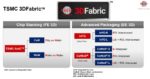
  • The full complement of SoIC, InFO, and CoWoS offerings have been incorporated into the TSMC “3D Fabric” product family, in anticipation of future system-level assemblies integrating both the 3D and 2.5D packaging technologies.

Introduction

Doug’s presentation covered the pillars of TSMC’s advanced packaging options:

  • the “front-end” SOIC die-to-die attach technology
  • the “back-end, chip-first” InFO (Integrated FanOut) technology
  • the “back-end, chip-last” CoWoS (Chip-on-Wafer-on-Substrate) technology

As will be discussed shortly, Doug announced several unique enhancements to the back-end options.

TSMC has grouped both the front-end and back-end options into a single package development roadmap, denoted as “3D Fabric”.  The last section of this article will illustrate how both these FE and BE technologies can be combined, into a complex 3D package solution.

SoIC

Background

SoIC technology enables direct die-to-die attach, using thermo-compression bonding between pads – here’s an earlier article that describes this process:  link.

Both face-to-face and face-to-back orientations are supported.  The face-to-back topology utilizes through silicon vias (TSVs) to provide the bonding pads.  TSVs also enable the addition of microbumps for subsequent package substrate attach.

(There is a variant of this technology that enables a highly efficient assembly flow, in the specific case where both die share the same footprint – “WoW’, for Wafer-on-Wafer.)

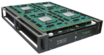
There are opportunities for integrating multiple die at the same level to the underlying base die (as in the figure above), as well as the capability to develop a vertical stack of thinned die.  The latter configuration is commonly used to construct high-bandwidth memory (HBM) stacks, with several memory die on top of a memory controller as the base.  Doug referenced a recently TSMC technical presentation illustrating a 12-high HBM stack (total thickness ~60um), utilizing the SoIC bonding technology.  (Reference:  Tsai, C.H., et al., “Low Temperature SoIC Bonding and Stacking Technology for 12/16-Hi High Bandwidth Memory (HBM)”, VLSI 2020 Symposium, Paper TH1.1.)

Advanced SoIC Development

  • thermal R (Tr)

An area of focus for SoIC development is the thermal resistance of the bond connections – it is critical that the heat generated within the die stack have a low Tr path to the package.  Doug’s presentation highlighted the continuous process improvement (CPI) activity that has reduced the bond Tr by ~25%.  (Similar CPI attention has been placed on reducing the Tr for microbump connections as well, by ~18%.)

  • bond pitch

Another major focus area is to scale the SoIC bond and TSV pitches, in conjunction with the areal density scaling of successive process nodes.  (If the bond and TSV pitch didn’t scale, that would adversely impact the realized density gains from migrating to the next node.)  Doug indicated the minimum bond and TSV pitches will indeed transition from 9um (N7) to 6um (N5) and to 4.5um (N3).  Doug also shared experimental data illustrating sub-um bond pitch reliability, for future node scaling.

Clearly, front-end SoIC packaging technology development is receiving considerable R&D investment.

InFO

Background

The Integrated FanOut technology utilizes a “back-end, chip-first” package assembly process.  As described in the earlier article mentioned above, InFO selects known good die and encapsulates them in a “reconstituted” wafer of an epoxy molding compound.

This enables the addition and patterning of dielectric and interconnect layers on top of the molding compound wafer to utilize existing fab equipment.  These interconnects, along with the final pattern of metal to the package attach microbumps, are collectively described as the redistribution layers (RDL).

As will be described shortly, TSMC is introducing alternative InFO technologies – the traditional InFO assembly with redistribution layers is now denoted as InFO-R.

There are other existing InFO designations – e.g., InFO-AIP with “antenna-in-package”, and InFO-PoP with “package-on-package”.  InFO-PoP integrates a chip stacked on top of the InFO assembly, whose microbumps attach to through-InFO vias (TIVs) in the molding compound to the RDL layers – see below.

The focus of the InFO package development presented at the Symposium was on enhancements to InFO-R, and a new InFO topology.

InFO-R Development

  • increasing reticle size

To enable greater flexibility in multi-die integration, TSMC has begun offering InFO assembly – e.g., die placement, encapsulation, and (specifically) RDL patterning – that exceeds the maximum photolithography reticle size.  The CoWoS technology has offered interconnect patterning on the silicon interposer that exceeds the 1X reticle size limit for some time;  this technique has recently been extended to InFO.  (1X maximum reticle size:  ~33mm x 26mm.)

Support for an InFO 1.7X reticle-size assembly will be available in 4Q20, with 2.5X in 1Q21 (qualified on a final package of 110mm x 110mm).  It is evident that there is significant customer demand for a low-cost package technology for ever-increasing multi-die configurations.

  • RDL interconnect

Key parameters for InFO-R are:  the die pad pitch to the RDL layers (40um), the RDL pitch (2um L/2um S), and the number of RDL layers (3).

Recently, TSMC R&D published an article describing development of sub-micron L/S patterning – more die in a large InFO-R assembly will require greater interconnect routing density.  (Reference:  Pu, et al., IEEE ECTC, 2018, p. 45-51.)

InFO-L

As mentioned above, the RDL line/space pitch is a key characteristics of the multi-die InFO assembly.  Yet, this dimension is limited by the processes available for the deposition, patterning, and curing of the organic dielectric and metallization used for the RDL layers.

To enable greater die-to-die routing capacity, TSMC is introducing a Local Silicon Interconnect (LSI) “bridge chiplet” embedded within the RDL assembly on top of the encapsulated die.  Compared to the baseline InFO-R technology, the embedded silicon bridge in InFO-L offers:

  • 25 um die pad pitch for LSI connectivity (versus 40um)
  • 0.4um/0.4um L/S (versus 2um/2um)
  • 4 metal layers (using TSMC’s “Mz” metal thickness process module)
  • InFO-L will be qualified in 1Q21, on a 1X reticle-size assembly

InFO-SoIS

The typical package substrate used with InFO-R provides connectivity from the InFO bumps to the package BGA balls, with limited interconnect layers within the substrate.   At the Symposium, TSMC shoed a unique variant of InFO-R, where the substrate consists of a composite of organic layers, providing 14 metal interconnect planes.  This demonstration of a “System-on-Integrated Substrate” may evolve to production status for a large-area, multi-die InFO-R assembly requiring more connectivity to BGA balls.
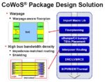
CoWoS

Background

The back-end, chip-last assembly known as Chip-on-Wafer-on-Substrate (CoWoS) technology has traditionally used a silicon interposer as the intermediate-level interconnect substrate for multi-die integration.  This option has been the mainstay for system implementations with an array of processor die, typically with multiple HBM memory stacks.

  • reticle size

Over the years, CoWoS technology development has focused on supporting increasing silicon interposer dimensions.  TSMC will be expanding the interposer size to 3X max reticle (2021) and 4X max reticle (2023), to support model processors and HBM stacks in the overall package.

  • improved interposer electrical characteristics

CoWoS process R&D has enabled the following enhancements:

– up to 5 Cu metal layers

– lower sheet resistivity (improving by 3X in 1H21)

– embedded capacitors

The traditional CoWoS topology with silicon interposer is now designated as CoWoS-S, to differentiate from the new configurations that Doug presented at the Symposium.

CoWoS-L

A new chip-last offering was introduced – CoWoS-L.  Like the embedded LSI interconnect bridge added to the InFO offering, a similar configuration is being added to the CoWoS assembly.  The silicon interposer is replaced by an organic substrate with an embedded LSI chiplet, offering interposer-like interconnect signal density in a more cost-effective assembly.

CoWoS-L plans are to provide:   1.5X reticle size (1 die, 4 HBM2E stacks), currently in production;  3X reticle size (3 die, 8 HBM2E stacks), in 2Q21.

Full Front-End (3D) and Back-End (2.5D) Integration

The 3D Fabric product initiative envisions a combination of (SoIC + InFO) and (SoIC + CoWoS) assemblies.  A multi-die, multi-tiered SoIC could be integrated as part of a (chip-first) encapsulated InFO offering.  An example is illustrated below of an SoIC integrated as part of a (chip-last) CoWoS assembly.

The full 3D Fabric offering is illustrated below.

In the 3D Fabric collection, note that there is also a CoWoS-R variant shown – a chip-last assembly on an organic substrate with RDL layers and no embedded LSI bridge.  Given the large number of wires required in the typical CoWoS die plus HBM stack topology, the embedded LSI bridge of CoWoS-L is likely required.  Here’s a cross-section of CoWoS-R.

TSMC has made a major investment in advanced packaging development – SoIC, InFO, and CoWoS have become an integral part of system architecture definition.  Increasingly, architects will need enhanced “pathfinding” tools to assist with the myriad of performance, power, area/volume, signal integrity, power delivery, thermal dissipation, reliability, and cost tradeoffs.

For more info on the full suite of 3D Fabric offerings, please follow this link.

-chipguy

Highlights of the TSMC Technology Symposium – Part 1

Highlights of the TSMC Technology Symposium – Part 3


In-Chip Monitoring Helps Manage Data Center Power

In-Chip Monitoring Helps Manage Data Center Power
by Tom Simon on 09-07-2020 at 6:00 am

in-chip sensing

Designers spend plenty of time analyzing the effects of process, voltage and temperature. But everyone knows it’s not enough to simply stop there. Operating environments are tough and have lots of limitations, especially when it comes to power consumption and thermal issues. Thermal protection and even over-voltage protections have been in chips for many years. However, there is more at stake than just preventing failures. It’s necessary to tune the operation of SoCs so they have long life and lower cost of operation, plus they need to stay within the limits of the cooling systems used in the facilities where they are located. In-chip monitoring can help manage power consumption and thermal issues.

This was a topic at the recent TSMC OIP event. Stephen Crosher, CEO of Moortec, a provider of IP for in-chip monitoring, presented on the topic of “Challenges of N5 HPC and Hyperscaling within Data Centers.” Small savings at the chip level in power consumption and heat generation translate into meaningful results when scaled up. Stephen points out that hyperscale data centers can have in the order of millions of SoCs.

Data centers already consume 1-2% of all electricity produced globally. Chinese data centers alone over the next 5 years are expected to use as much electricity as all of Australia. Data center traffic and workloads are expected to rise by 80% over the next 3 years.

The only way to effectively manage power is to design in feedback systems to manage SoC operation so that they minimize the power. The first step in doing this is to ensure there is accurate and complete information about all three of process, voltage and temperature. With the right kind of in-chip monitoring capabilities many things can be done inside of an SoC to respond to each of these conditions.

Stephen provides examples of how tightening the voltage monitoring precision at the terminus of the supply nets from 5% to 1% can reduce supply guard banding and reduce power by ~10%. Multiplied across millions of chips, fractions of a penny per hour per chip translate into savings of millions of dollars per year. Likewise, for thermal management, more accurate sensors can prevent premature device throttling. Moortec’s ‘out-of-the-box’ high accuracy sensors can help avoid unnecessary throttling when compared to more alternative +/- 5% sensors, especially with considering that Moortec sensors can achieve even high accuracies if calibration can be accommodated in production test.

N5 is an appealing process for high performance chips. It offers around a 15% speed improvement along with an 80% greater logic density. It also reduces power consumption. However, at the same time the power density per square mm is going up. So dynamic voltage and frequency scaling will increasingly be important for managing energy consumption and thermal behavior. Stephen points out that for every watt saved on-chip, there is a commensurate reduction in facility cooling costs. Hyperscale data centers spend 40% of their operating costs on cooling, so there is even more incentive to lower server power use.

The future of in-chip monitoring looks very interesting with telemetry facilitating reporting and analysis. Some of the benefits could include enhanced device screening, power optimization, increased performance and extended reliability. Many of the benefits can go beyond large data centers and find their way into automotive, consumer and other applications. Moortec has been developing in-chip monitoring solutions since 2010 and have ample experience on a wide range of process nodes, including the most advanced. The presentation was eye opening as far as the impacts of chip level optimizations on facility, enterprise and even worldwide economies and environmental impact.