S2C has been developing FPGA prototyping platforms since 2003, and, over time, their FPGA prototyping platforms have supported increasingly larger more sophisticated FPGA prototyping projects with three key attributes; 1) scalable prototyping gate capacities, 2) a high-speed interface between the FPGA prototype and software running on a host computer, and 3) support for globally distributed users. A natural evolution of these three FPGA prototyping attributes has led S2C to produce its latest FPGA prototyping platform dubbed the “Prodigy Cloud System”.
Hyperscale SoC Validation Gate Capacity – Driven by customer demand for what S2C calls “Hyperscale SoC Validation”, S2C’s Prodigy Cloud System now supports very large SoC prototyping requirements up to 2 billion gates (“Hyper”) in a modularly scalable way … hence “Hyperscale”. To achieve Hyperscale capabilities, S2C has harnessed the latest and largest Intel FPGA called the Stratix 10 GX 10M FPGA. This Intel FPGA blows away all other FPGAs generally available today with an estimated usable gate capacity of 80M gates per FPGA. The GX 10M FPGA is fabricated with Intel’s 14nm silicon, so its expected to run faster and consume less power. Intel acknowledges in its GX 10M FPGA press release1 that “One market in particular has a critical interest in always using the largest available FPGAs: the ASIC prototyping and emulation market.” Intel sees FPGA emulation and prototyping supporting a variety of system development tasks including;
- Algorithm development using real hardware
- Early SoC software development prior to the chip’s manufacture
- RTOS verification
- Corner-case condition testing for both hardware and software
- Regression testing on successive design iterations
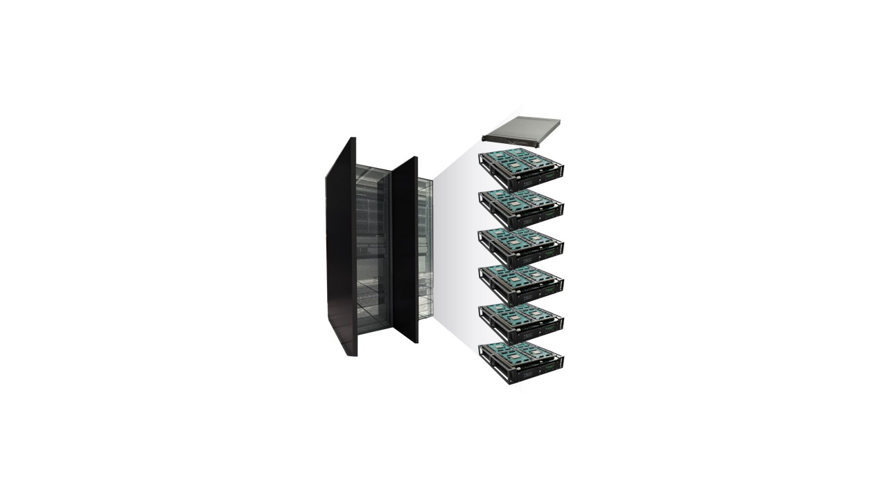
The S2C Prodigy Cloud System comes in a standard server rack and can scale up to eight (8) Quad 10M Logic Systems, each with four (4) GX 10M FPGAs, so one server rack can house up to 32 GX 10M FPGAs. With an estimated 80 million gates per FPGA, the Prodigy Cloud System should easily support 2 billion gates for FPGA prototyping! And, if that’s not enough gate capacity, multiple server racks can be connected together.
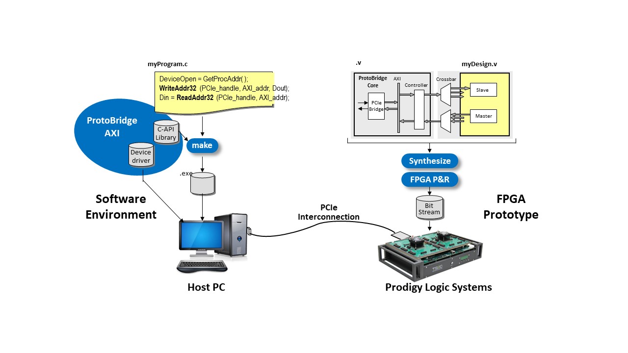
 Fast Interface to Simulation Environment – The second key attribute of the Prodigy Cloud System is an out-of-the-box hardware and software solution for applying large quantities of real-world test data in the form of bus traffic, communications traffic, video images, etc. to the FPGA prototype from your host computer. This approach creates what S2C calls a “simulation infrastructure” that enables the user to connect the SoC hardware model in the FPGA to a simulation-like verification environment on the host computer.
S2C calls this option ProtoBridge, and it includes PCIe bridge and AXI master/slave logic that is compiled and downloaded into the FPGA together with the SoC prototype design. The host computer connects to the FPGA prototype with a PCI cable that supports up to 1GB/s transfers, and ProtoBridge includes PCI driver software, and a set of C-API function calls to drive AXI bus transactions from the host computer. Global Remote Access and Control – The third key attribute of the Prodigy Cloud System is support for multiple globally distributed users. Large SoC design teams today may be spread across multiple locations in the US, Europe, China, India, and Vietnam, so remote access to the FPGA prototyping resources is essential for an optimal ROI from the prototyping investment.
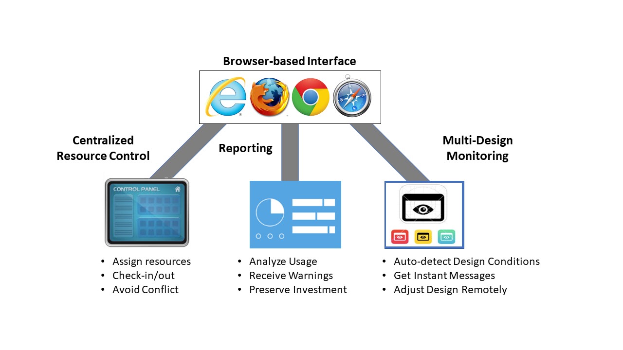
To address this key attribute, S2C has developed what it calls Prodigy Neuro hardware and software. The Prodigy Neuro hardware, called the Prodigy Neuro Control Module, manages global power control to the FPGA hardware, clocks and resets, self-test, and monitoring of the Prodigy Cloud System FPGA board connections.
Prodigy Neuro Software provides centralized control of the Prodigy Cloud System hardware resources, as well as user and prototyping project management. Prodigy Neuro Software includes a browser-based GUI for easy remote access to Prodigy Cloud System hardware for centralized resource control and multi-design management and monitoring. Prodigy Cloud System hardware can be allocated to multiple different projects running simultaneously on the hardware, with 3-level permission control for multiple users. Prodigy Neuro Software also provides FPGA prototyping hardware usage analytics, warnings of hardware faults, and auto-detection of hardware connection with instant messaging upon first check-in. So, if you thought that your SoC designs were too large for FPGA prototyping, or you needed a shareable FPGA prototyping resource for a globally distributed design team and multiple FPGA prototyping projects, you should register for this webinar. You will get a copy of the replay if you can’t attend the live broadcast.
Also Read:
WEBINAR: Prototyping With Intel’s New 80M Gate FPGA
S2C Delivers FPGA Prototyping Solutions with the Industry’s Highest Capacity FPGA from Intel!
Share this post via:


Comments
There are no comments yet.
You must register or log in to view/post comments.