webinar banner AI 2026 v2

Reverse-engineering the First FPGA Chip Xilinx XC2064

Reverse-engineering the First FPGA Chip Xilinx XC2064
by Ken Shirriff on 09-16-2020 at 6:00 am

Xilinx XC2064

A Field-Programmable Gate Array (FPGA) can implement arbitrary digital logic, anything from a microprocessor to a video generator or crypto miner. An FPGA consists of many logic blocks, each typically consisting of a flip flop and a logic function, along with a routing network that connects the logic blocks. What makes an FPGA special is that it is programmable hardware: you can redefine each logic block and the connections between them. The result is you can build a complex digital circuit without physically wiring up individual gates and flip flops or going to the expense of designing a custom integrated circuit.

Die photo closeup showing the circuitry for one of the 64 tiles in the XC2064 FPGA. The metal layers have been removed, exposing the silicon and polysilicon transistors underneath. Click for a larger image. From siliconpr0n.


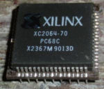
The FPGA was invented by Ross Freeman1 who co-founded Xilinx2 in 1984 and introduced the first FPGA, the XC2064. 3 This FPGA is much simpler than modern FPGAs—it contains just 64 logic blocks, compared to thousands or millions in modern FPGAs—but it led to the current multi-billion-dollar FPGA industry. Because of its importance, the XC2064 is in the Chip Hall of Fame. I reverse-engineered Xilinx’s XC2064, and in this blog post I explain its internal circuitry (above) and how a “bitstream” programs it.

The Xilinx XC2064 was the first FPGA chip. Photo from siliconpr0n.


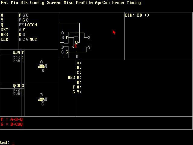
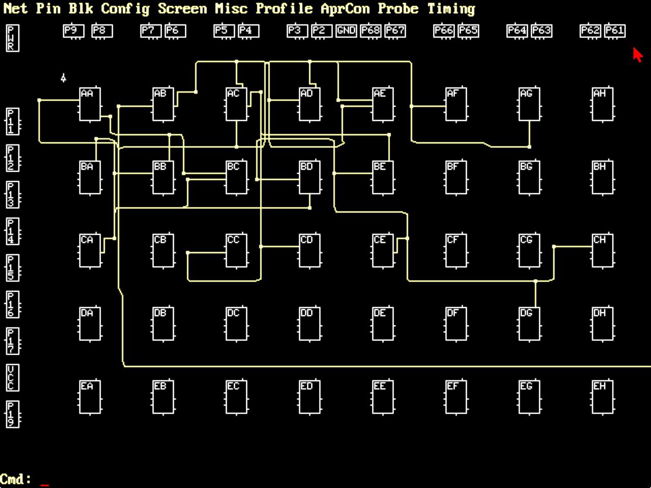
Nowadays, an FPGA is programed in a hardware description language such as Verilog or VHDL, but back then Xilinx provided their own development software, an MS-DOS application named XACT with a hefty $12,000 price tag. XACT operated at a lower level than modern tools: the user defined the function of each logic block, as shown in the screenshot below, and the connections between logic blocks. XACT routed the connections and generated a bitstream file that could be loaded into the FPGA.

Screenshot of XACT. The two lookup tables F and G implement the equations at the bottom of the screen, with Karnaugh map shown above.


An FPGA is configured via the bitstream, a sequence of bits with a proprietary format. If you look at the bitstream for the XC2064 (below), it’s a puzzling mixture of patterns that repeat irregularly with sequences scattered through the bitstream. There’s no clear connection between the function definitions in XACT and the data in the bitstream. However, studying the physical circuitry of the FPGA reveals the structure of the bitstream data and it can be understood.

Part of the bitstream generated by XACT.


How does an FPGA work?

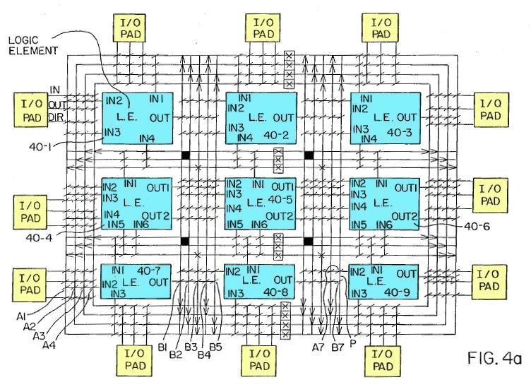
The diagram below, from the original FPGA patent, shows the basic structure of an FPGA. In this simplified FPGA, there are 9 logic blocks (blue) and 12 I/O pins. An interconnection network connects the components together. By setting switches (diagonal lines) on the interconnect, the logic blocks are connected to each other and to the I/O pins. Each logic element can be programmed with the desired logic function. The result is a highly programmable chip that can implement anything that fits in the available circuitry.

The FPGA patent shows logic blocks (LE) linked by an interconnect.


CLB: Configurable Logic Block

While the diagram above shows nine configurable logic blocks (CLBs), the XC2064 has 64 CLBs. The diagram below shows the structure of each CLB. Each CLB has four inputs (A, B, C, D) and two outputs (X and Y). In between is combinatorial logic, which can be programmed with any desired logic function. The CLB also contains a flip flop, allowing the FPGA to implement counters, shift registers, state machines and other stateful circuits. The trapezoids are multiplexers, which can be programmed to pass through any of their inputs. The multiplexers allow the CLB to be configured for a particular task, selecting the desired signals for the flip flop controls and the outputs.

A Configurable Logic Block in the XC2064, from the datasheet.

You might wonder how the combinatorial logic implements arbitrary logic functions. Does it select between a collection of AND gates, OR gates, XOR gates, and so forth? No, it uses a clever trick called a lookup table (LUT), in effect holding the truth table for the function. For instance, a function of three variables is defined by the 8 rows in its truth table. The LUT consists of 8 bits of memory, along with a multiplexer circuit to select the right value. By storing values in these 8 bits of memory, any 3-input logic function can be implemented.4

The interconnect

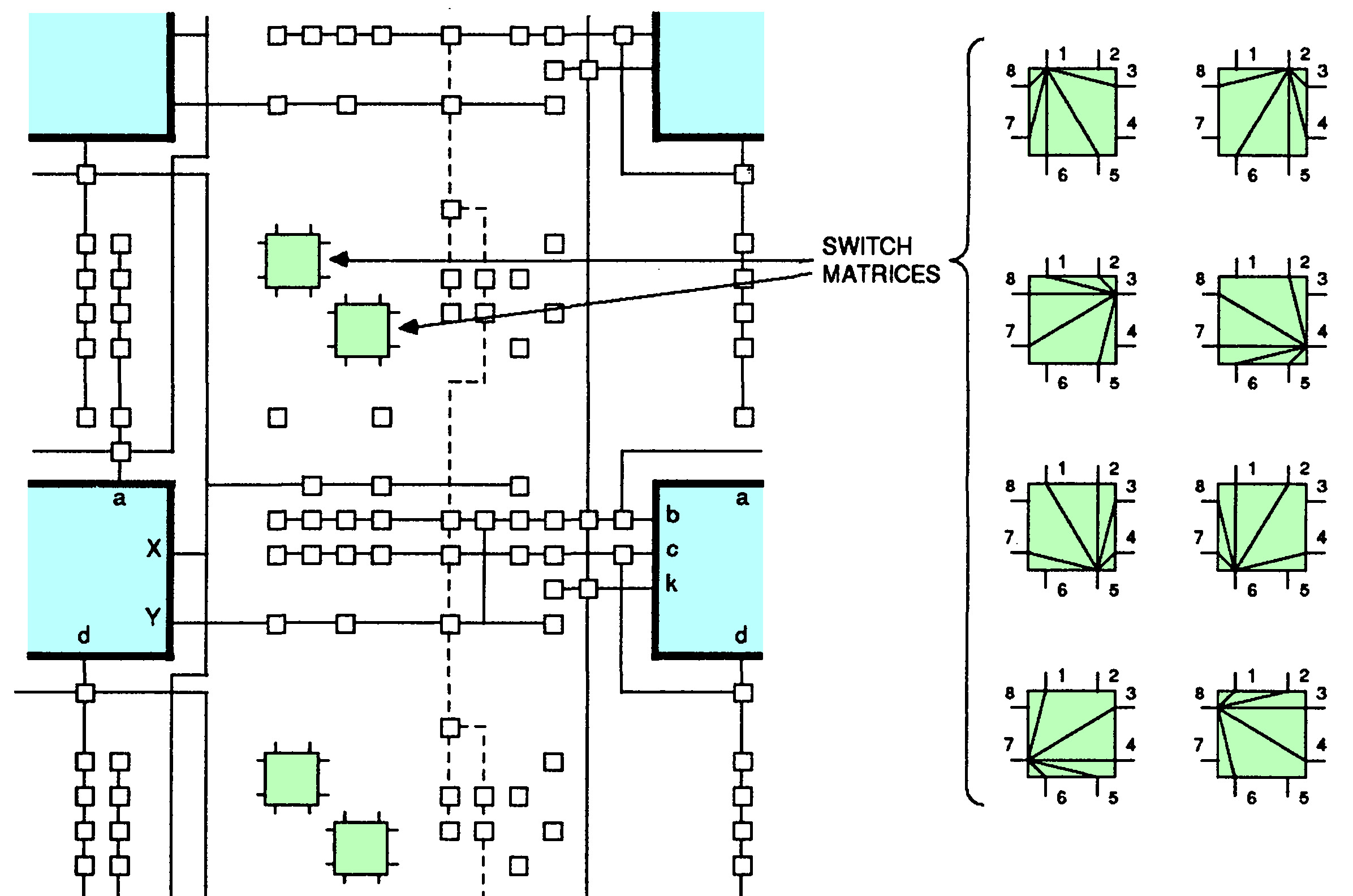
The second key piece of the FPGA is the interconnect, which can be programmed to connect the CLBs in different ways. The interconnect is fairly complicated, but a rough description is that there are several horizontal and vertical line segments between each CLB. CLB. Interconnect points allow connections to be made between a horizontal line and a vertical line, allowing arbitrary paths to be created. More complex connections are done via “switch matrices”. Each switch matrix has 8 pins, which can be wired together in (almost) arbitrary ways.

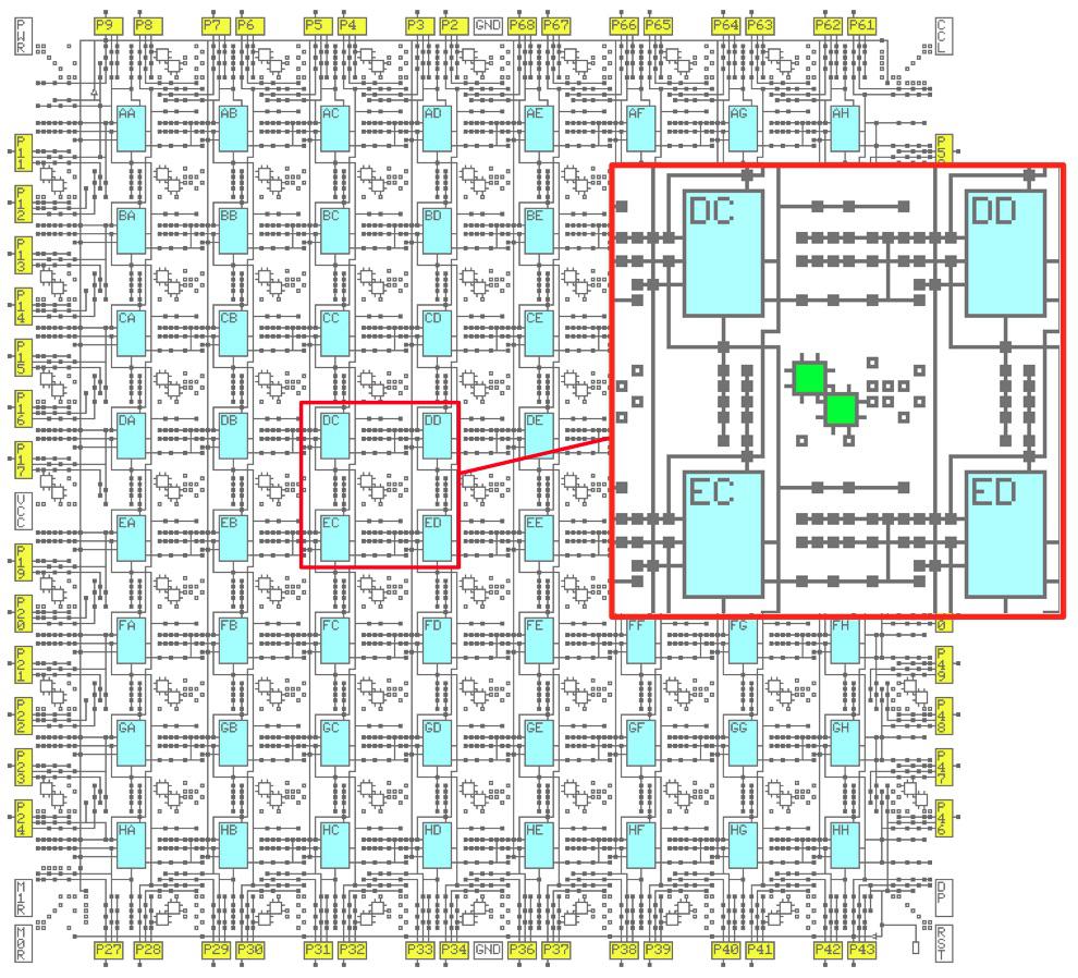
The diagram below shows the interconnect structure of the XC2064, providing connections to the logic blocks (cyan) and the I/O pins (yellow). The inset shows a closeup of the routing features. The green boxes are the 8-pin switch matrices, while the small squares are the programmable interconnection points.

The XC2064 FPGA has an 8 by 8 grid of CLBs. Each CLB has an alphabetic name from AA to HH.


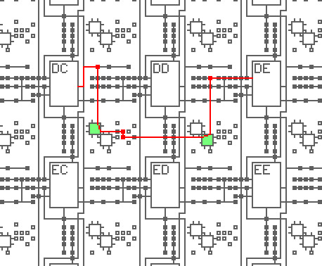
The interconnect can wire, for example, an output of block DC to an input of block DE, as shown below. The red line indicates the routing path and the small red squares indicate activated routing points. After leaving block DC, the signal is directed by the first routing point to an 8-pin switch (green) which directs it to two more routing points and another 8-pin switch. (The unused vertical and horizontal paths are not shown.) Note that routing is fairly complex; even this short path used four routing points and two switches.

Example of a signal routed from an output of block DC to block DE.


The screenshot below shows what routing looks like in the XACT program. The yellow lines indicate routing between the logic blocks. As more signals are added, the challenge is to route efficiently without the paths colliding. The XACT software package performs automatic routing, but routes can also be edited manually.

Screenshot of the XACT program. This MS-DOS program was controlled via the keyboard and mouse.


The implementation

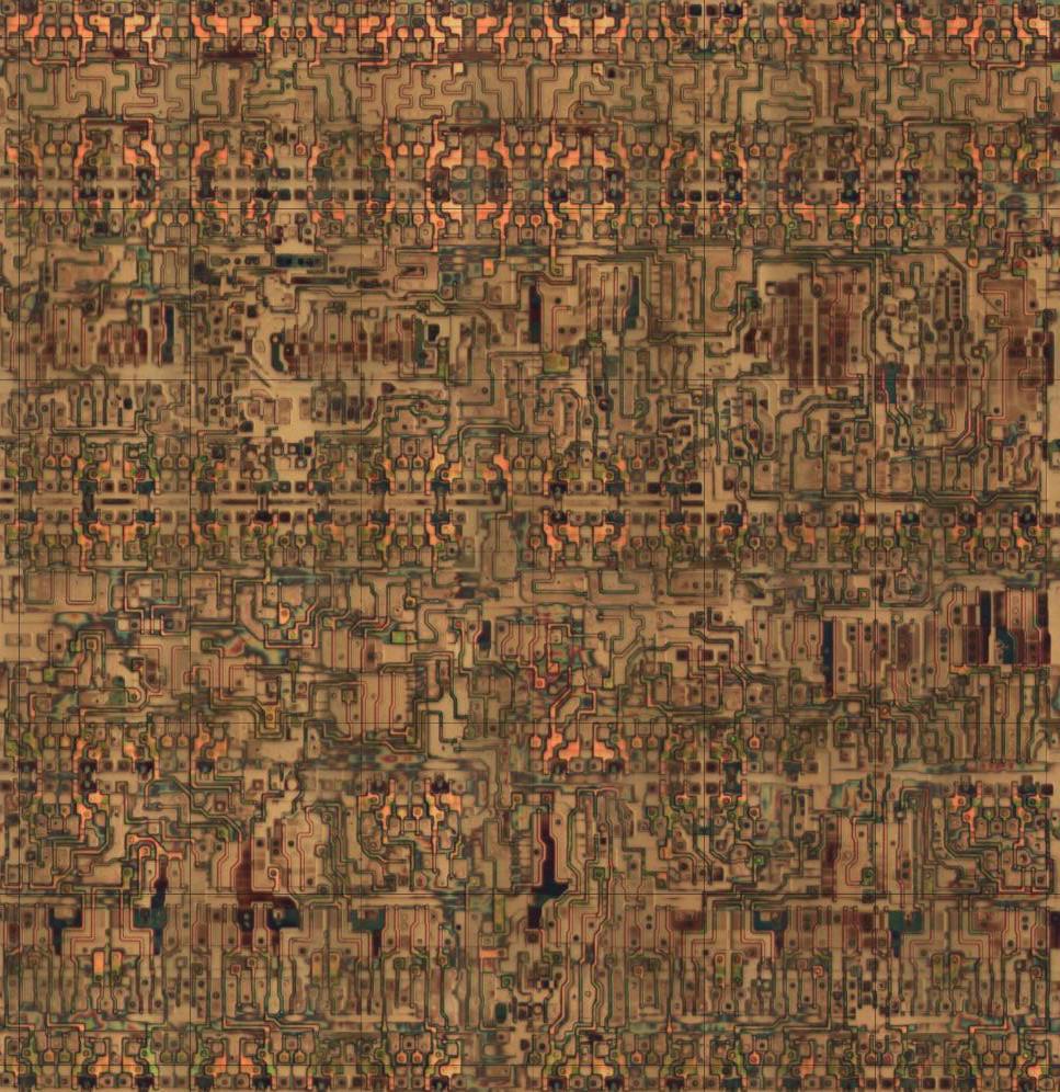
The remainder of this post discusses the internal circuitry of the XC2064, reverse-engineered from die photos.5 Be warned that this assumes some familiarity with the XC2064.

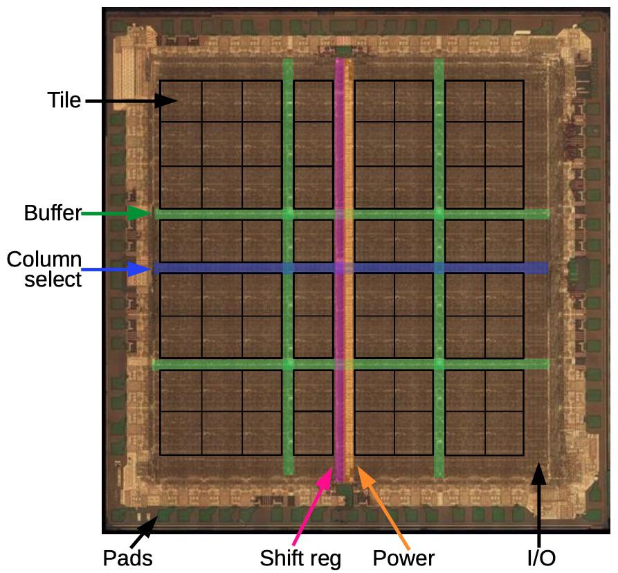
The die photo below shows the layout of the XC2064 chip. The main part of the FPGA is the 8×8 grid of tiles; each tile holds one logic block and the neighboring routing circuitry. Although FPGA diagrams show the logic blocks (CLBs) as separate entities from the routing that surrounds them, that is not how the FPGA is implemented. Instead, each logic block and the neighboring routing are implemented as a single entity, a tile. (Specifically, the tile includes the routing above and to the left of each CLB.)

Layout of the XC2064 chip. Image from siliconpr0n.


Around the edges of the integrated circuit, I/O blocks provide communication with the outside world. They are connected to the small green square pads, which are wired to the chip’s external pins. The die is divided by buffers (green): two vertical and two horizontal. These buffers amplify signals that travel long distances across the circuit, reducing delay. The vertical shift register (pink) and horizontal column select circuit (blue) are used to load the bitstream into the chip, as will be explained below.

Inside a tile

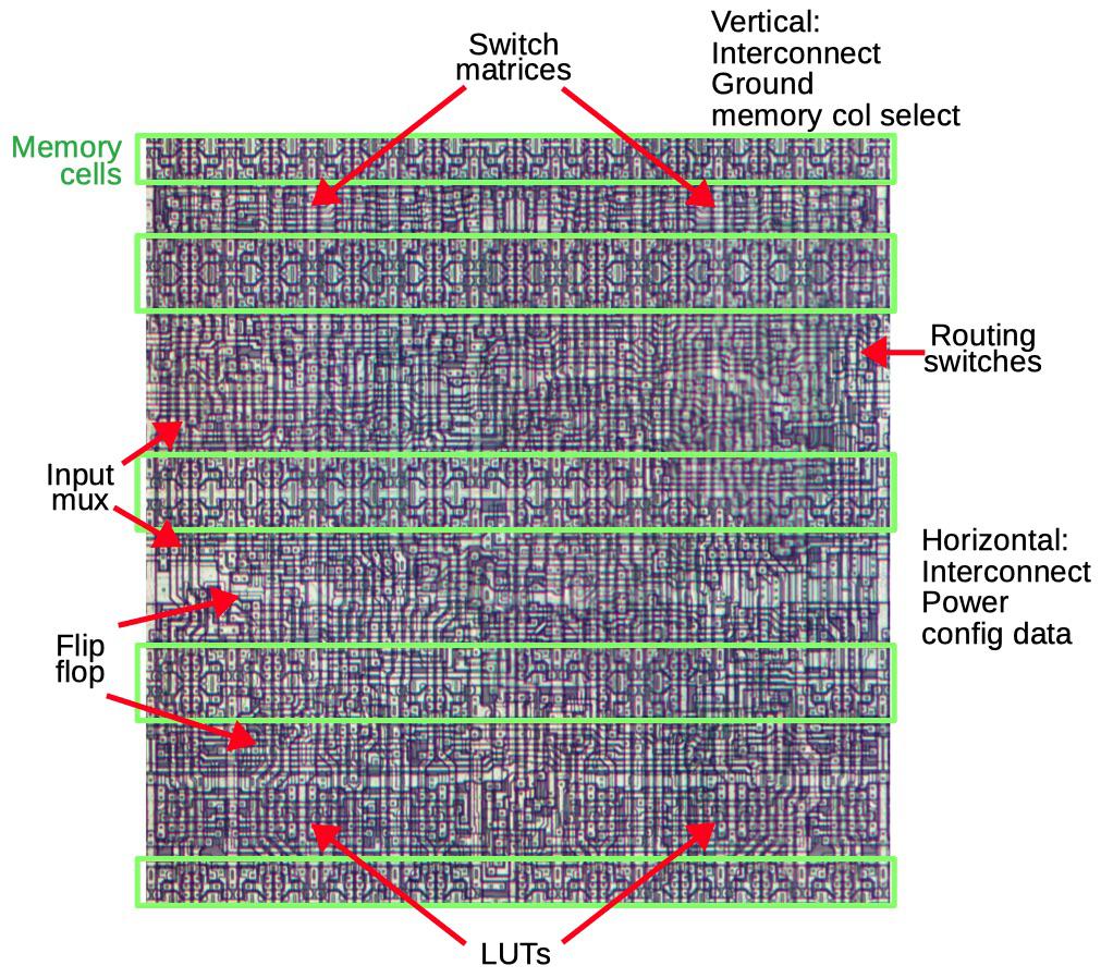
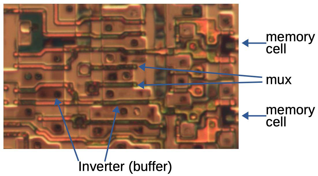
The diagram below shows the layout of a single tile in the XC2064; the chip contains 64 of these tiles packed together as shown above. About 40% of each tile is taken up by the memory cells (green) that hold the configuration bits. The top third (roughly) of the tile handles the interconnect routing through two switch matrices and numerous individual routing switches. Below that is the logic block. Key parts of the logic block are multiplexers for the input, the flip flop, and the lookup tables (LUTs). The tile is connected to neighboring tiles through vertical and horizontal wiring for interconnect, power and ground. The configuration data bits are fed into the memory cells horizontally, while vertical signals select a particular column of memory cells to load.

One tile of the FPGA, showing important functional units.


Transistors

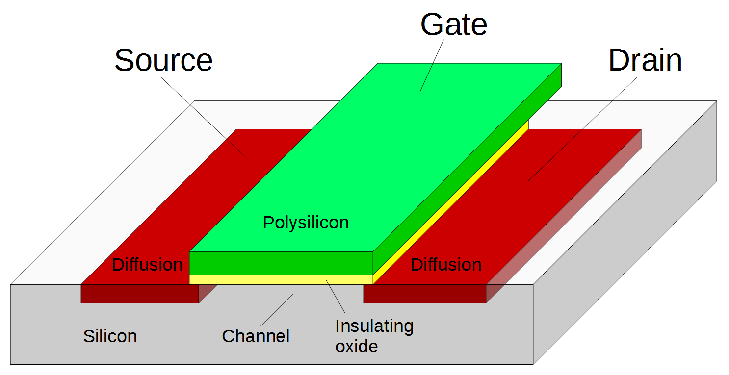
The FPGA is implemented with CMOS logic, built from NMOS and PMOS transistors. Transistors have two main roles in the FPGA. First, they can be combined to form logic gates. Second, transistors are used as switches that signals pass through, for instance to control routing. In this role, the transistor is called a pass transistor. The diagram below shows the basic structure of an MOS transistor. Two regions of silicon are doped with impurities to form the source and drain regions. In between, the gate turns the transistor on or off, controlling current flow between the source and drain. The gate is made of a special type of silicon called polysilicon, and is separated from the underlying silicon by a thin insulating oxide layer. Above this, two layers of metal provide wiring to connect the circuitry.

Structure of a MOSFET.


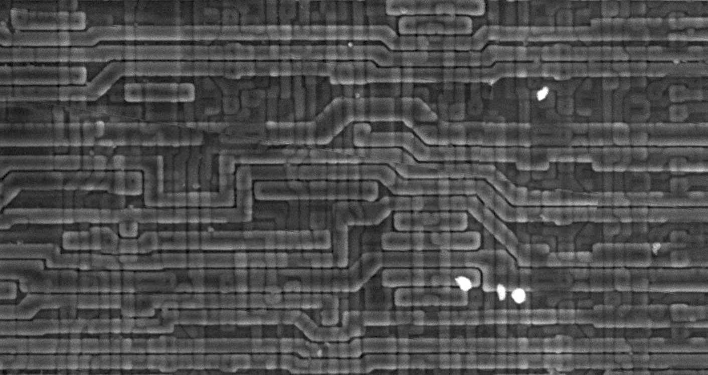
The die photo closeup below shows what a transistor looks like under a microscope. The polysilicon gate is the snaking line between the two doped silicon regions. The circles are vias, connections between the silicon and the metal layer (which has been removed for this photo).

A MOSFET as it appears in the FPGA.


The bitstream and configuration memory

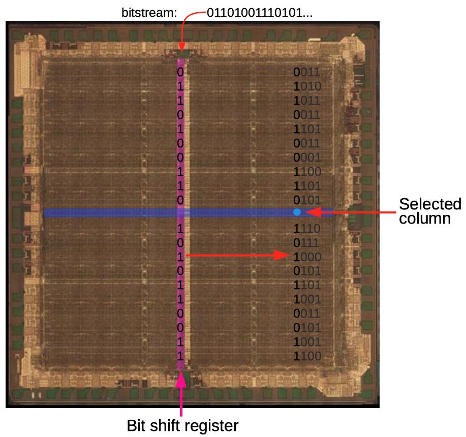
The configuration information in the XC2064 is stored in configuration memory cells. Instead of using a block of RAM for storage, the FPGA’s memory is distributed across the chip in a 160×71 grid, ensuring that each bit is next to the circuitry that it controls. The diagram below shows how the configuration bitstream is loaded into the FPGA. The bitstream is fed into the shift register that runs down the center of the chip (pink). Once 71 bits have been loaded into the shift register, the column select circuit (blue) selects a particular column of memory and the bits are loaded into this column in parallel. Then, the next 71 bits are loaded into the shift register and the next column to the left becomes the selected column. This process repeats for all 160 columns of the FPGA, loading the entire bitstream into the chip. Using a shift register avoids bulky memory addressing circuitry.

How the bitstream is loaded into the FPGA. The bits shown are conceptual; actual bit storage is much denser. The three columns on the left have been loaded and the fourth column is currently being loaded. Die photo from siliconpr0n.


The important point is that the bitstream is distributed across the chip exactly as it appears in the file: the layout of bits in the bitstream file matches the physical layout on the chip. As will be shown below, each bit is stored in the FPGA next to the circuit it controls. Thus, the bitstream file format is directly determined by the layout of the hardware circuits. For instance, when there is a gap between FPGA tiles because of the buffer circuitry, the same gap appears in the bitstream. The content of the bitstream is not designed around software concepts such as fields or data tables or configuration blocks. Understanding the bitstream depends on thinking of it in hardware terms, not in software terms.7

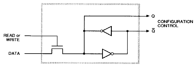
Each bit of configuration memory is implemented as shown below.8 Each memory cell consists of two inverters connected in a loop. This circuit has two stable states so it can store a bit: either the top inverter is 1 and the bottom is 0 or vice versa. To write to the cell, the pass transistor on the left is activated, passing the data signal through. The signal on the data line simply overpowers the inverters, writing the desired bit. (You can also read the configuration data out of the FPGA using the same path.) The Q and inverted Q outputs control the desired function in the FPGA, such as closing a routing connection, providing a bit for a lookup table, or controlling the flip flops. (In most cases, just the Q output is used.)

Schematic diagram of one bit of configuration memory, from the datasheet. Q is the output and Q is the inverted output.


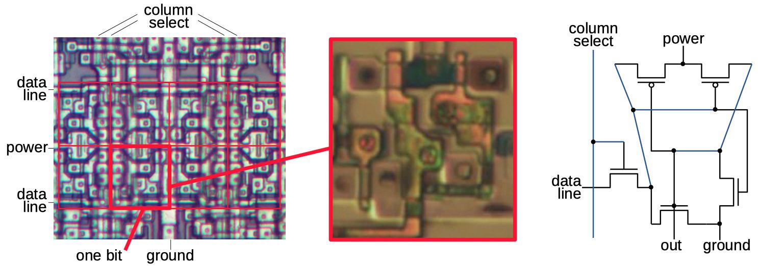
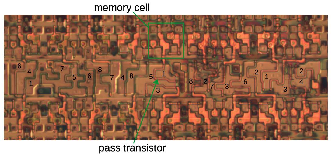
The diagram below shows the physical layout of memory cells. The photo on the left shows eight memory cells, with one cell highlighted. Each horizontal data line feeds all the memory cells in that row. Each column select line selects all the memory cells in that column for writing. The middle photo zooms in on the silicon and polysilicon transistors for one memory cell. The metal layers were removed to expose the underlying transistors. The metal layers wire together the transistors; the circles are connections (vias) between the silicon or polysilicon and the metal. The schematic shows how the five transistors are connected; the schematic’s physical layout matches the photo. Two pairs of transistors form two CMOS inverters, while the pass transistor in the lower left provides access to the cell.

Eight bits of configuration memory, four above and four below. The red box shows one bit. When a column select line is activated, the row data line is loaded into the corresponding cells. The closeup and schematic show one bit of configuration memory. Die photo from siliconpr0n.


Lookup table multiplexers

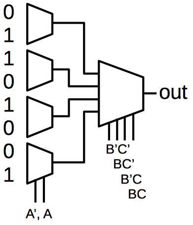
As explained earlier, the FPGA implements arbitrary logic functions by using a lookup table. The diagram below shows how a lookup table is implemented in the XC2064. The eight values on the left are stored in eight memory cells. Four multiplexers select one of each pair of values, depending on the value of the A input; if A is 0, the top value is selected and if A is 1 the bottom value is selected. Next, a larger multiplexer selects one of the four values based on B and C. The result is the desired value, in this case A XOR B XOR C. By putting different values in the lookup table, the logic function can be changed as desired.

Implementing XOR with a lookup table.


Each multiplexer is implemented with pass transistors. Depending on the control signals, one of the pass transistors is activated, passing that input to the output. The diagram below shows part of the LUT circuitry, multiplexing two of the bits. At the right are two of the memory cells. Each bit goes through an inverter to amplify it, and then passes through the multiplexer’s pass transistors in the middle, selecting one of the bits.

A closeup of circuitry in the LUT implementation. Die photo from siliconpr0n.


Flip flop

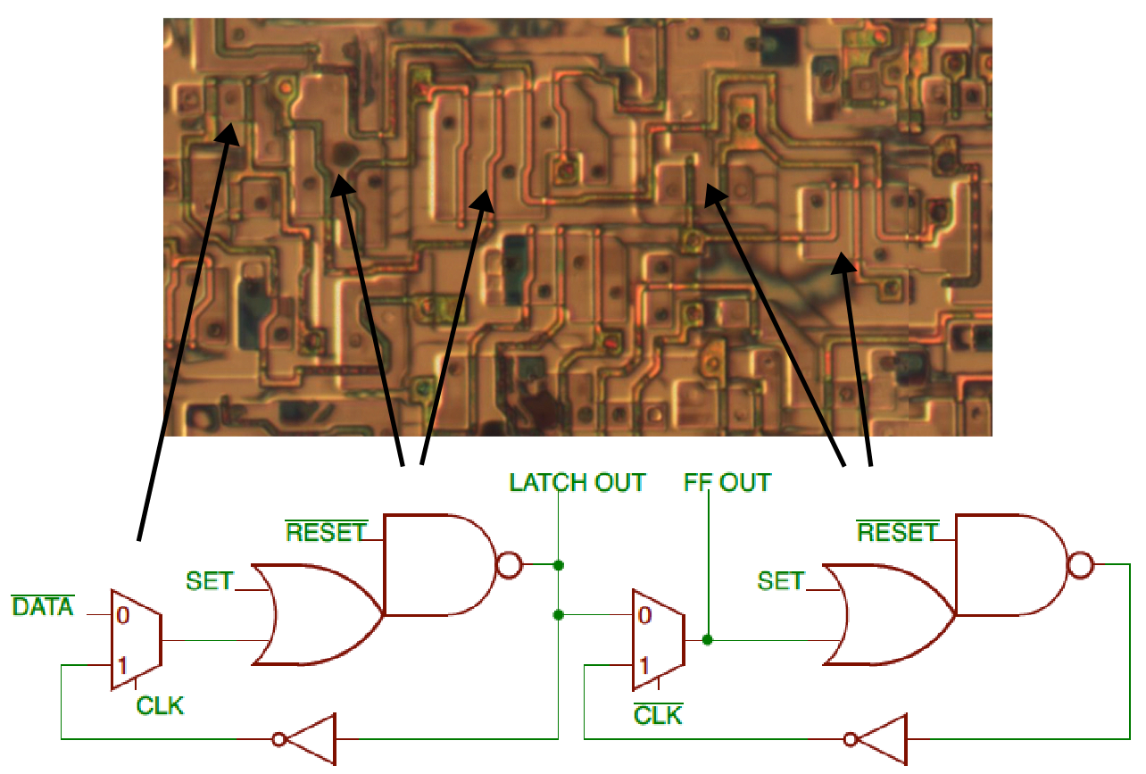
Each CLB contains a flip flop, allowing the FPGA to implement latches, state machines, and other stateful circuits. The diagram below shows the (slightly unusual) implementation of the flip flop. It uses a primary/secondary design. When the clock is low, the first multiplexer lets the data into the primary latch. When the clock goes high, the multiplexer closes the loop for the first latch, holding the value. (The bit is inverted twice going through the OR gate, NAND gate, and inverter, so it is held constant.) Meanwhile, the secondary latch’s multiplexer receives the bit from the first latch when the clock goes high (note that the clock is inverted). This value becomes the flip flop’s output. When the clock goes low, the secondary’s multiplexer closes the loop, latching the bit. Thus, the flip flop is edge-sensitive, latching the value on the rising edge of the clock. The set and reset lines force the flip flop high or low.

Flip flop implementation. The arrows point out the first multiplexer and the two OR-NAND gates. Die photo from siliconpr0n.


8-pin switch matrix

The switch matrix is an important routing element. Each switch has eight “pins” (two on each side) and can connect almost any combination of pins together. This allows signals to turn, split, or cross over with more flexibility than the individual routing nodes. The diagram below shows part of the routing network between four CLBs (cyan). The switch matrices (green) can be connected with any combination of the connections on the right. Note that each pin can connect to 5 of the 7 other pins. For instance, pin 1 can connect to pin 3 but not pin 2 or 4. This makes the matrix almost a crossbar, with 20 potential connections rather than 28.


The switch matrix is implemented by a row of pass transistors controlled by memory cells above and below. The two sides of the transistor are the two switch matrix pins that can be connected by that transistor. Thus, each switch matrix has 20 associated control bits;9 two matrices per tile yields matrix 40 control bits per tile. The photo below indicates one of the memory cells, connected to the long squiggly gate of the pass transistor below. This transistor controls the connection between pin 5 and pin 1. Thus, the bit in the bitstream corresponding to that memory cell controls the switch connection between pin 5 and pin 1. Likewise, the other memory cells and their associated transistors control other switch connections. Note that the ordering of these connections follows no particular pattern; consequently, the mapping between bitstream bits and the switch pins appears random.

Implementation of an 8-pin switch matrix. The silicon regions are labeled with the corresponding pin numbers. The metal layers (which connect the pins to the transistors) were removed for this photo. Based on die photo from siliconpr0n.


Input routing

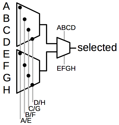
The inputs to a CLB use a different encoding scheme in the bitstream, which is explained by the hardware implementation. In the diagram below, the eight circled nodes are potential inputs to CLB box DD. Only one node (at most) can be configured as an input, since connecting two signals to the same input would short them together.

Input selection. The eight nodes circled in green are potential inputs to DD; one of them can be selected.


The desired input is selected using a multiplexer. A straightforward solution would use an 8-way multiplexer, with 3 control bits selecting one of the 8 signals. Another straightforward solution would be to use 8 pass transistors, each with its own control signal, with one of them selecting the desired signal. However, the FPGA uses a hybrid approach that avoids the decoding hardware of the first approach but uses 5 control signals instead of the eight required by the second approach.

The FPGA uses multiplexers to select one of eight inputs.


The schematic above shows the two-stage multiplexer approach used in the FPGA. In the first stage, one of the control signals is activated. The second stage picks either the top or bottom signal for the output.10 For instance, suppose control signal B/F is sent to the first stage and ‘ABCD’ to the second stage; input B is the only one that will pass through to the output. Thus, selecting one of the eight inputs requires 5 bits in the bitstream and uses 5 memory cells.

Conclusion

The XC2064 uses a variety of highly-optimized circuits to implement its logic blocks and routing. This circuitry required a tight layout in order to fit onto the die. Even so, the XC2064 was a very large chip, larger than microprocessors of the time, so it was difficult to manufacture at first and cost hundreds of dollars. Compared to modern FPGAs, the XC2064 had an absurdly small number of cells, but even so it sparked a revolutionary new product line.

Two concepts are the key to understanding the XC2064’s bitstream. First, the FPGA is implemented from 64 tiles, repeated blocks that combine the logic block and routing. Although FPGAs are described as having logic blocks surrounded by routing, that is not how they are implemented. The second concept is that there are no abstractions in the bitstream; it is mapped directly onto the two-dimensional layout of the FPGA. Thus, the bitstream only makes sense if you consider the physical layout of the FPGA.

I’ve determined how most of the XC2064 bitstream is configured (see footnote 11) and I’ve made a program to generate the CLB information from a bitstream file. Unfortunately, this is one of those projects where the last 20% takes most of the time, so there’s still work to be done. One problem is handling I/O pins, which are full of irregularities and their own routing configuration. Another problem is the tiles around the edges have slightly different configurations. Combining the individual routing points into an overall netlist also requires some tedious graph calculations.

I announce my latest blog posts on Twitter, so follow me at kenshirriff for updates. I also have an RSS feed. Thanks to John McMaster, Tim Ansell and Philip Freidin for discussions.12

Notes and references

  1. Ross Freeman tragically died of pneumonia at age 45, five years after inventing the FPGA. In 2009, Freeman was recognized as the inventor of the FPGA by the Inventor’s Hall of Fame
  2. Xilinx was one of the first fabless semiconductor companies. Unlike most semiconductor companies that designed and manufactured semiconductors, Xilinx only created the design while a fab company did the manufacturing. Xilinx used Seiko Epson Semiconductor Division (as in Seiko watches and Epson printers) for their initial fab. 
  3. Custom integrated circuits have the problems of high cost and the long time (months or years) to design and manufacture the chip. One solution was Programmable Logic Devices (PLD), chips with gate arrays that can be programmed with various functions, which were developed around 1967. Originally they were mask-programmable; the metal layer of the chip was designed for the desired functionality, a new mask was made, and chips were manufactured to the specifications. Later chips contained a PROM that could be “field programmed” by blowing tiny fuses inside the chip to program it, or an EPROM that could be reprogrammed. Programmable logic devices had a variety of marketing names including Programmable Logic ArrayProgrammable Array Logic (1978), Generic Array Logic and Uncommitted Logic Array. For the most part, these devices consisted of logic gates arranged as a sum-of-products, although some included flip flops. The main innovation of the FPGA was to provide a programmable interconnect between logic blocks, rather than a fixed gate architecture, as well as logic blocks with flip flops. For an in-depth look at FPGA history and the effects of scalability, see Three Ages of FPGAs: A Retrospective on the First Thirty Years of FPGA Technology. Also see A Brief History of FPGAs
  4. The lookup tables in the XC2064 are more complex than just a table. Each CLB contains two 3-input lookup tables. The inputs to the lookup tables in the XC2064 have programmable multiplexers, allowing selection of four different potential inputs. In addition, the two lookup tables can be tied together to create a function on four variables or other combinations.
    Logic functions in the XC2064 FPGA are implemented with lookup tables. From the datasheet.


  5. To analyze the XC2064, I used my own die photos of the XC20186 as well as the siliconpr0n photos of the XC2064 and XC2018. Under a light microscope, the FPGA is hard to analyze because it has two metal layers. John McMaster used his electron microscope to help disambiguate the two layers. The photo below shows how the top metal layer is emphasized by the electron microscope.
    Electron microscope photo of the XC2064, courtesy of John McMaster.


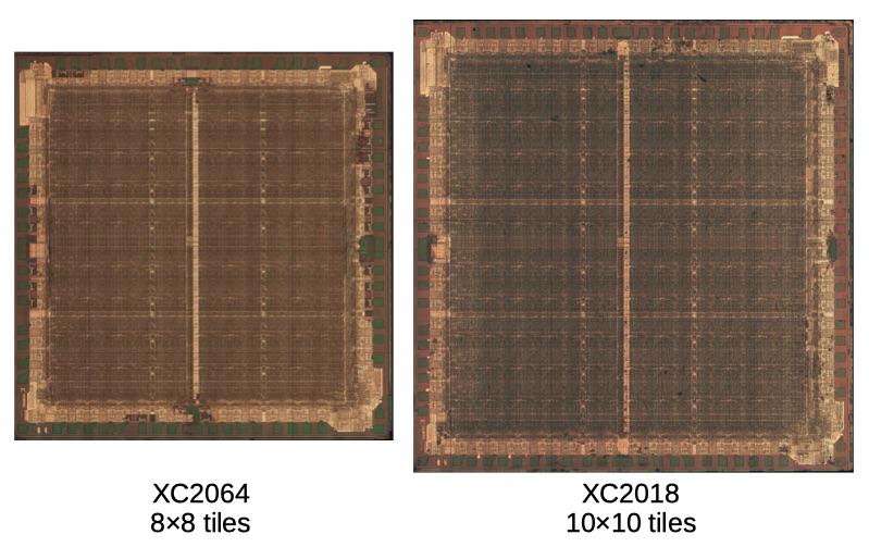
  6. The Xilinx XC2018 FPGA (below) is a 100-cell version of the XC2064 FPGA. Internally, it uses the same tiles as the 64-cell XC2064, except it has a 10×10 grid of tiles instead of an 8×8 grid. The bitstream format of the XC2018 is very similar, except with more entries.
    The Xilinx XC2018 FPGA. On the right, the lid has been removed, showing the silicon die. The tile pattern is faintly visible on the die.


    The image below compares the XC2064 die with the XC2018 die. The dies are very similar, except the larger chip has two more rows and columns of tiles.

    Comparison of the XC2064 and XC2018 dies. The images are scaled so the tile sizes match; I don’t know how the physical sizes of the dies compare. Die photos from siliconpr0n.


  7. While the bitstream directly maps onto the hardware layout, the bitstream file (.RBT) does have a small amount of formatting, shown below.
    The format of the bitstream data, from the datasheet.


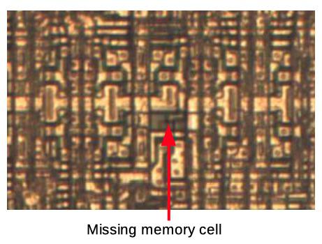
  8. The configuration memory is implemented as static RAM (SRAM) cells. (Technically, the memory is not RAM since it must be accessed sequentially through the shift register, but people still call it SRAM.) These memory cells have five transistors, so they are known as 5T SRAM.One question that comes up is if there are any unused bits in the bitstream. It turns out that many bits are unused. For instance, each tile has an 18×8 block of bits assigned to it, of which 27 bits are unused. Looking at the die shows that the memory cell for an unused bit is omitted entirely, allowing that die area to be used for other circuitry. The die photo below shows 9 implemented bits and one missing bit.

    Memory cells, showing a gap where one cell is missing. Die photo from siliconpr0n.


  9. The switch matrix has 20 pass transistors. Since each tile is 18 memory cells wide, two of the transistors are connected to slightly more distant memory cells. 
  10. A few notes on the CLB input multiplexer. The control signal EFGH is the complement of ABCD, so only one control signal is needed in the bitstream and only one memory cell for this signal. Second, other inputs to the CLB have 6 or 10 choices; the same two-level multiplexer approach is used, changing the number of inputs and control signals. Finally, a few of the control signals are inverted (probably because the inverted memory output was closer). This can cause confusion when trying to understand the bitstream, since some bits appear to select 6 inputs instead of 2. Looking at the complemented bit, instead, restores the pattern. 
  11. The following table summarizes the meaning of each bit in a tile’s 8×18 part of the bitstream. Each entry in the table corresponds to one bit in the bitstream and indicates what part of the FPGA is controlled by that bit. Empty entries indicate unused bits. 


    #2: 1-3 #2: 3-4 PIP D2,D5 (bit inverted) Gin_3 = D G = 1 2′ 3′
    #2: 1-2 #2: 2-6 #2: 2-4 PIP A2,A5 (bit inverted) Gin_3 = C G = 1′ 2′ 3′
    #2: 3-7 #2: 3-6 PIP D3, D4, D5 PIP A3, A4, A5 G = 1′ 2 3′
    #2: 2-7 #2: 2-8 ND 11 PIP A1, A4 G = 1 2 3′
    #2: 1-5 #2: 3-5 PIP A3, AX PIP D1, D4 Y=F G = 1 2′ 3
    #2: 4-8 #2: 5-8 ND 10 PIP D3, DX Y=G Gin_2 = B G = 1′ 2′ 3
    #2: 7-8 #2: 6-8 ND 9 PIP B2, B5, B6, BX, BY PIP Y2 X=G Gin_1 = A G = 1′ 2 3
    #2: 5-6 #2: 5-7 ND 8 PIP B3,BX (bit inverted) PIP Y4 X=F G = 1 2 3
    #2: 4-6 #2: 1-4 #2: 1-7 PIP C1, C3, C4, C7 PIP X3 Q = LATCH Base FG (separate LUTs)
    #1: 3-5 #1: 5-8 #1: 2-8 PIP X2
    #1: 3-4 #1: 2-4 ND 7 PIP C3,CX (bit inverted) PIP X1 Fin_1 = A F = ! 1 2 3
    #1: 1-2 #1: 1-3 ND 6 PIP B6, B7 CLK = enabled Fin_2 = B F = 1′ 2 3
    #1: 1-5 #1: 1-4 ND 5 PIP C6, C7 CLK = inverted (FF), noninverted (LATCH) F = 1′ 2′ 3
    #1: 4-8 #1: 4-6 ND 4 PIP C4, C5 CLK = C F = 1 2′ 3
    #1: 2-7 #1: 1-7 ND 3 PIP B4, B5 PIP K1 SET = F F = 1 2 3′
    #1: 2-6 #1: 3-6 ND 2 PIP B2, BC PIP K2 SET = none F = 1′ 2 3′
    #1: 7-8 #1: 3-7 ND 1 PIP C1, C2 PIP Y3 RES = D or G Fin_3 = C F = 1′ 2′ 3′
    #1: 6-8 #1: 5-6 #1: 5-7 PIP B1, BY PIP Y1 RES = G Fin_3 = D F = 1 2′ 3′

    The first two columns of the table indicate the switch matrices. There are two switch matrices, labeled #1 (red) and #2 (green) in my diagram below. The 8 pins on matrix #1 are labeled 1-8 clockwise. (Switch #2 is the same, but there wasn’t room for the labels.) For example, “#2: 1-3” indicates that bit connects pins 1 and 3 on switch #2. The next column defines the “ND” non-directional connections, the boxes below with purple numbers near the switch matrices. Each ND bit in the table controls the corresponding ND connection.

    Diagram of the interconnect showing the numbering scheme I made up for the bitstream table.


    The next two columns describe what I’m calling the PIP connections, the solid boxes on lines above. The connections from output X (brown) are controlled by individual bits (X1, X2, C3). Likewise, the connections from output Y (yellow). The connections to input B (light purple) are different. Only one of these input connections can be active at a time, so they are encoded with multiple bits using the multiplexer scheme. Inputs C (cyan), D (blue) and A (green) are similar. The remaining table columns describe the CLB; refer to the datasheet for details. Bits control the clock, set and reset lines. The X and Y outputs can be selected from the F or G LUTs. The last two columns define the LUTs. There are three inputs for LUT F and three inputs for LUT G, with multiplexers controlling the inputs. Finally, the 8 bits for each LUT are defined, specifying the output for a particular combination of three inputs. 

  12. Various FPGA patents provide some details on the chips: 4870302464248747062164758985, and RE34363. XACT documentation was formerly at Xilinx, but they seem to have removed it. It can now be found here. John McMaster has some xc2064 tools available. 

GLOBALFOUNDRIES Goes Virtual with 2020 Global Technology Conference Series!

GLOBALFOUNDRIES Goes Virtual with 2020 Global Technology Conference Series!
by Daniel Nenni on 09-15-2020 at 10:00 am

GTC 400x400 1

GlobalFoundries is one of the more interesting semiconductor stories of this decade. They started as a spinout of the AMD fabs then acquired Chartered Semiconductor Manufacturing in 2009 and the IBM Microelectronics business in 2014.

Now that events are virtual it is a great time for my fellow semiconductor professionals to get an update on GF and other big players in the ecosystem. The talk with Arm CEO Simon Seagers should be an interesting one, absolutely.

Unlike some semiconductor events this one is open to all of us and I hope to see you there!

Engaging events with a sharp focus on industry challenges, innovations on the horizon and opportunities to accelerate the digital future

Santa Clara, Calif., September 14, 2020 – GLOBALFOUNDRIES® (GF®) today announced it will launch its Global Technology Conferences (GTC) 2020 series virtually with their first event, GTC North America on September 24. The one-day conference, themed ‘Accelerating the Digital Future’, is an opportunity for hundreds of customers and industry experts to engage and gain insight into how GF is helping to shape the digital transformation with the latest approaches and solutions for AI, IoT and 5G.

“Semiconductors play a vital role in our lives now more than ever, presenting both opportunities and challenges for our industry,” said Juan Cordovez, senior vice president of Global Sales at GF. “GLOBALFOUNDRIES’ GTC 2020 provides a virtual, interactive platform to spotlight thought leaders, inspire critical thinking, and to bring together customers and partners to showcase the latest innovations that will accelerate the digital future.”

To kick off the virtual conference, CEO Tom Caulfield will share his perspective on how geopolitical forces and the COVID-19 pandemic have unleashed global changes and opportunities for our industry and examine how GF’s solutions are enabling key megatrends that will reshape the world and enable a better normal.

Additionally, Tom will engage in real conversations with top industry leaders, including:
· Steve Mollenkopf, Qualcomm CEO
· Simon Segars, Arm CEO
· Lip-Bu Tan, Cadence CEO
· John Neuffer, SIA President and CEO

At GTC North America, more than 30 sessions with leading visionaries, technologists and partners will detail future trends in AI, silicon photonics and 6G, explore the latest opportunities in audio, analog power, AI, 5G and wireless connectivity and discover new offerings to simplify design cycle and accelerate time to market. Additionally, attendees will have access to GF’s virtual exhibit hall, providing a place to connect and engage with GF experts and more than 30 ecosystem event sponsors. Platinum sponsors for GTC 2020 include Analog Bits, Cadence Design Systems, Mentor and Synopsys. Gold sponsors are Arm, Advanced Semiconductor Engineering, Inc. (ASE Group) and VeriSilicon.

The GTC series will continue throughout October and November with additional events in Europe, China and Taiwan, each featuring a unique lineup of industry leaders and panel discussions.

For more information and to view the agenda or register for GF’s North America Global Technology Conference visit: https://bit.ly/354jbSp. Follow the latest conference updates on social media via #GFGTC2020 on Twitter, LinkedIn, and Facebook.

About GTC
GLOBALFOUNDRIES’ annual Global Technology Conference series features keynotes from industry leaders and presentations from senior members of the GF management and technical teams, with a special emphasis on how the company achieves time-to-volume leadership by leveraging global collaboration with customers and partners. On September 24, GTC 2020 North America kicks off a series of international events including Europe, Taiwan and Singapore. For more information on GTC 2020, visit: https://gf.swoogo.com/gtc2020northamerica/

About GF
GLOBALFOUNDRIES (GF) is the world’s leading specialty foundry. GF delivers differentiated feature-rich solutions that enable its customers to develop innovative products for high-growth market segments. GF provides a broad range of platforms and features with a unique mix of design, development and fabrication services. With an at-scale manufacturing footprint spanning the U.S., Europe and Asia, GF has the flexibility and agility to meet the dynamic needs of clients across the globe. GF is owned by Mubadala Investment Company. For more information, visit www.globalfoundries.com.

ONEGFTogether

Erica McGill
GLOBALFOUNDRIES| Corporate Communications
O: 518.305.5978 | M: 518.795.5240

Also Read:

Designing AI Accelerators with Innovative FinFET and FD-SOI Solutions

Contact over Active Gate Process Requirements for 5G

Embedded MRAM for High-Performance Applications


AI in Korea. Low-Key PR, Active Development

AI in Korea. Low-Key PR, Active Development
by Bernard Murphy on 09-15-2020 at 6:00 am

korea ai min

Based on press coverage and technical paper volume, you could be forgiven for thinking that Korea had decided to take a pass on AI mania, or maybe just to dabble a little here and there to stay abreast of trends. But you’d be wrong. Korea is very active in AI; they don’t feel a need to trumpet what they’re doing from the rooftops. If you dig around, there are plenty of hints. I talked with Kurt Shuler of Arteris IP to get a better understanding. I’m talking here about AI hardware, of course.

According to Kurt, most of the development action is between the Samsung Advanced Institute of Technology (SAIT), Seoul National University (SNU), and the government-funded Korea Institute of Advanced Science and Technology (KAIST), with substantial application development and competition among subsidiaries of the Samsung chaebol, which in part explains the lack of high-profile PR. Lots of internal development and competition, little entrepreneurial development outside those ecosystems.

Automotive AI

There is some activity outside these three. Hyundai and Kia do joint development. For example, they recently announced a Smart Cruise Control device that learns from the driver’s normal patterns how to adjust in a way comfortable to that driver. They base this on the fusion of sensing from cameras and radar. I couldn’t find information on ASIC support, but it’s not a stretch to assume Samsung played a significant role.

There’s an automotive Tier 1 in Korea called Hyundai Mobis which offers ADAS products, certainly within Korea, though aiming to be a worldwide supplier. They offer lane-keeping, smart cruise control (see above), autonomous emergency braking, highway driving assistance and autonomous parking. Again, unclear who is doing what in this development, but there’s no reason to believe the major IP depends on anyone outside Korea.

A  startup

I was also able to find one startup, Furiosa (inspired by the movie Mad Max: Fury Road), by founders with backgrounds from Samsung, KAIST, Qualcomm and AMD. They have $7M in seed round funding from Korean investors, have built an FPGA prototype and expect to have first silicon this year.

Samsung

The bulk of the development Kurt sees is in Samsung and is predominantly applied engineering and applied research rather than core research. Arteris IP works with a number of these groups. Where is it going? Remember Samsung is massively vertically integrated. They make smartphones, of course, that need AI horsepower. But they also make TVs, fridges, other appliances, each of which has been adding AI capabilities like voice recognition. They’re not hiding this progress; they’re just not competing for attention in the “who has the biggest and baddest AI engine” race. It’s all about internal applications, from applied research, to chips, to consumer products, robotics, and industry 4.0 products.

On the flip side, SemiWiki readers know Samsung as one of the major semiconductor foundries. Samsung is very active in using AI for fundamental research in that area, to discover new materials they could use to advance semiconductor manufacturing. Along these lines, they recently announced discovery of a material called amorphous boron-nitride.

AI investment

In other recent news, the Korean government said recently that it plans to invest nearly $1B over the next ten years to advance the next generation of semiconductor development, including cutting edge AI. And Samsung reported that it plans to add 1,000 staff in AI this year.

So yeah, Korea is active in AI. They’re just not banging any drums about it. You can learn more about why so many of these groups are using the Arteris IP NoC interconnect technology HERE.

Also Read:

CEO Interview: Charlie Janac of Arteris IP

Interconnect Basics: Wires to Crossbar to NoC

Where’s the Value in Next-Gen Cars?


Trusted IoT Ecosystem for Security – Created by the GSA and Chaired by Mentor/Siemens

Trusted IoT Ecosystem for Security – Created by the GSA and Chaired by Mentor/Siemens
by Mike Gianfagna on 09-14-2020 at 10:00 am

MentorSiemens and the GSA Team to Create a Trusted IoT Ecosystem

There’s a lot to keep you awake at night these days. If you live in California, it’s wildfires and unbreathable air. If you live on planet Earth, it’s COVID-19. And if you’re part of the value chain for IoT, it’s the security and robustness of the silicon and software fabric that connects our world. This fabric connects everything, from autonomous vehicles to the power grid to the world economy. And it’s vulnerable. A compromised piece of hardware or software can cause real damage and potential loss of life. This extends to the cloud and the data used for AI/ML. This is why the Global Semiconductor Alliance (GSA) created the collaborative Trusted IoT Ecosystem for Security (TIES) Group with Mentor/Siemens as Board Chair with board members NXP, Rambus, Microsoft and Arm.

In my opinion, creating a trusted, secure ecosystem to source the silicon and software for our current and future interconnected world is not an optional item. Rather it is a requirement for continued innovation, robust growth and a safe future. Let’s start with a look at one of the founders of this movement along with the GSA.

The Mentor/Siemens Vision

Siemens is a huge multi-national technology corporation. Electrification, automation and digitization (EAD) is a central theme for much of what Siemens does. Mentor now lives in Siemens Digital Industries, creating near-perfect synergy to tackle the challenges of the IoT ecosystem. A recent article entitled A Stroke of Genius That Saved the Day: Siemens’ Purchase of Mentor lays out the details of the Mentor synergy. 

At Embedded World in 2019, Intel and Siemens delivered a joint showcase for Intel® Secure Device Onboard (SDO) and SIMATIC IPCs. Using Siemens MindSphere®, which is an industrial IoT as a service solution along with Intel® Secure Device Onboard provisioning service, a reduced cost and more robust system enabling a zero-touch mass deployment of devices was demonstrated.

This, in turn led to a three-way collaboration for a proof of concept project using Intel SDO with the Infineon TPM chip as root-of-trust for onboarding SIMATIC IPCs to MindSphere or other platforms. This demonstrates how a trusted ecosystem collaboration can be created to deliver end-to-end solutions across a variety of domains in the IoT value chain.

Secure Device Onboard (SDO) is now open source software via a Linux Foundation Edge project, and SDO technology is now migrating into an industry standard as part of a FIDO Alliance IoT initiative. A draft spec is now publicly available.

The GSA Reach

Addressing the challenges of creating a trusted IoT ecosystem requires a lot of companies to align. System OEMs, software development, design, IP, manufacturing, assembly and test along with cloud and edge applications are all involved. The problem has substantial scale. It turns out the GSA is a near perfect catalyst to bring all the key stakeholders together in one unified, focused setting.  Its members represent 70% of the $450B+ semiconductor industry and include fundamental technology companies representing all major segments of the semiconductor ecosystem.

The Plan

Recently, I had a chance to chat with Tom Katsioulas. Tom is the Board Chair of the GSA TIES Group and the Head of TrustChain at Mentor, a Siemens Business. He has been working with the GSA to create the vision, charter and process to start tackling the work needed to create a trusted IoT ecosystem. Tom explained that a plan has been developed and is being circulated to the GSA membership.

This is very encouraging. With the right support, momentum from positive results and addition of new members from the broader system community, the GSA can expand its footprint and help solve a very important problem in the chip-to-cloud IoT value chain. New ecosystem members, from OEMs, to IC and PCB, to embedded system, to device, to edge applications, to digital twins are all needed.

Tom explained that the objective of this work is to promote trusted end-to-end solutions in the IoT value chain that accelerate the adoption, growth and field use of connected chips, devices, systems and IoT applications. Enabling recurring services revenue streams and high value business models is also a focus. Ambitious goals for sure, but ones that have the significant vision and support from the GSA TIES Group.

The operating model for the program is illustrated by the figure on the right.  The process builds on itself with continued successful application to a growing list of end-to-end use cases that drive collaborative solutions and guidelines in the IoT value chain.

The output of these activities will be provided to the relevant parties (including standards organizations) for potential action and implementation. Tom explained that there are organizations usually in need of a well-defined problem statement with clear goals, use cases, examples and a group of companies to support the work. The GSA Trusted IoT Ecosystem Security Group can provide all this and promote any best practices developed.

Call to Action

Ecosystems capture higher value than sum of members acting independently, and trust is essential for collaboration. A number of companies are committing to contribute content for the effort. If you are a member of the GSA, you will have the opportunity to participate in this important initiative. If you’re not a GSA member, you can still participate. Either way, get involved and contribute. You may well be helping to save the planet.

You can learn more about this Trusted IoT Ecosystem for Security here. You can also contact Shungo Saito: SSaito@gsaglobal.org. Shungo is the director, program development at GSA.

Also Read:

Emulation as a Service Benefits New AI Chip

WEBINAR: Addressing Verification Challenges in the Development of Optimized SRAM Solutions with surecore and Mentor Solido

Creating Analog PLL IP for TSMC 5nm and 3nm


CEO Interview: Pengwei Qian of SkillCAD

CEO Interview: Pengwei Qian of SkillCAD
by Daniel Nenni on 09-14-2020 at 6:00 am

IMG 4723

Pengwei Qian is the founder and CEO of SkillCAD, a grassroots EDA company that has amassed the most impressive customer list (60+ companies) I have experienced for a company of this size, absolutely.

Pengwei has a Bachelor’s degree in Physics and a Masters in Material Science from Fudan University and a Masters in Electronic Engineering from National University of Singapore. He started as an IC designer and now has more than 20 years of experience in EDA. Pengwei is also the co-founder of MiniSilicon and founder of YAMMI Inc.

 Why did you start SkillCAD?
When I was a CAD engineer for Elantec (acquired by Intersil) I saw that layout design required many repetitive mouse clicks, even for simple tasks.  As IC design became more complex so did the use of highly repetitive commands which significantly reduced layout team productivity while increasing the number of design errors and tape-out delays.  I felt that if tedious, repetitive, layout tasks could be simplified and automated it would reduce design time and increase the layout quality of results.

But the automation could not come at the expense of loss of control by the layout designer.  The type of custom layout design required by sophisticated Radio Frequency (RF), Power Management (PM), and many other complicated Mixed-Signal applications requires that the experienced layout designer maintain complete control of the design outcome.  The focus of SkillCAD has always been to create commands to automate complex layout tasks so that the designer can focus on the critical thought processes needed to create high quality layout.

How does SkillCAD integrate with the Cadence Virtuoso Layout Suite?
As the name implies, SkillCAD is a collection of layout commands written in the SKILL programming language. The SkillCAD IC Layout Automation Suite (IC LAS) seamlessly integrates into the Cadence Virtuoso layout design environment, using the layout and rule files supplied by the Cadence system. Since the tools were developed to support the native Cadence library objects they can be used in compliment to the Cadence tools. The levels of simplification and automation afforded by the SkillCAD commands can improve layout productivity by more than 50%. Cadence Virtuoso plus SkillCAD IC LAS have become the preferred layout environment for analog, RF and mixed signal designs.

What are the benefits of using SKILLCAD?
In the past internal CAD groups have independently written SKILL based tools for layout teams but rarely do they have the number of proven commands that are found  in IC LAS.  SkillCAD works closely with the top semiconductor companies and foundries integrating the latest design practices and process technologies. It really is a collaborative software product with many years of experience embedded into it.

Can you provide more detail on that?
Sure, SkillCAD commands have been used in production IC design for more than 12 years and have been developed in response to requests by layout designers around the world who are experts in the field and know what they need to increase their productivity and accuracy.

The commands are inspired by dedicated semiconductor professionals and implemented in innovative ways. SkillCAD’s proprietary “correct and optimized by construction” commands eliminate design rule violations, automates complex error prone layout implementation, and significantly improves a layout team’s productivity.

SkillCAD tools are maintained and supported by our SKILL programming experts, who are also knowledgeable on the needs of layout designers. This relieves CAD teams, often under-manned and over-tasked, of the burdens of trying to develop and maintain tools specific to layout teams or semiconductor manufacturing technologies.  The initial setup required for SkillCAD IC LAS is minimal and can be done for each manufacturing process. Today SkillCAD IC LAS works with Cadence Virtuoso Platforms: IC5, IC6, IC12 and IC18.

Who is the typical customer of SkillCAD IC LAS?
SkillCAD commands are designed to support all levels of the layout design flow and adapt to the design methodologies of most layout teams and individuals. Today our 120+ commands target custom mixed signal, RF and analog designs for process nodes at 12nm and above. We do have customers using IC LAS for advanced FinFET processes down to 3nm which will be fully supported in the upcoming release.

What are some of the issues associated with advanced process nodes as it relates to Layout design?
What makes designing at 10nm and below difficult is the increased complexity that comes from the additional physical design rules and constraints required for the additional metal layers and EUV technology.  Advanced nodes also require that Layout teams must now incorporate sophisticated color-aware custom routing and color aware physical design layout.

To better understand the upcoming layout challenges SkillCAD works very closely with advanced node customers and foundries to develop new commands and features to provide the automation needed to insure their layout teams can handle the increased complexity and shorten time to tape-out.

Where are you located and can you tell me a little more about your company?
We are located at 1580 Old Oakland Road, San Jose CA. We have been a Cadence connection partner since 2008.  We have distributors in Japan, China, Erupoe, Taiwan and Korea.  Feel free to visit our website to learn more: www.SkillCAD.com.   Should you want to view our 120 commands with tutorials and videos just click on the link below.  www.SkillCAD.com/reference-guide.   If you would like a demo or download an eval license please contact us at support@SkillCAD.com.

Also Read:

CEO Interview: Charlie Janac of Arteris IP

CEO Interview: Anna Fontanelli of Monozukuri

CEO Interview: Isabelle Geday of Magillem


VLSI Symposium 2020 – Imec Monolithic CFET

VLSI Symposium 2020 – Imec Monolithic CFET
by Scotten Jones on 09-13-2020 at 10:00 am

th311591894514842 Page 04

The 2020 VLSI Technology Symposium was held as a virtual conference from June 14th through June 19th. At the symposium Imec gave an interesting paper on Monolithic CFET and I had a chance to interview one of the authors, Hiroaki Arimura.

It is well known in the industry that FinFETs (FF) are reaching the end of their scaling life. Samsung has already announced that they are moving to Horizontal Nanosheets (HNS) at 3nm. TSMC is staying with FF at 3nm but is expected to move to a new architecture for 2nm. Intel is expected to stay with FF at 7nm and then move to HNS at 5nm, assuming they are still pursuing their own technology at that point.

The most likely roadmap for the industry is FF to HNS with or without Forksheets, and then to transition to Complimentary FETs (CFET), see figure 1.

Figure 1. Imec CMOS Roadmap.

 The forksheet and CFET provide shrinks by improving the n to p spacing with CFETs stacking nFET and pFET devices, see figure 2.

Figure 2. CFET structure.

 In the current work a “monolithic” CFET has been developed by using separate wafers for the nFET and pFET and then bonding them together versus a “sequential” CFET where both FET types are fabricated on the same wafer. Imec claims that the monolithic technique is less expensive than the sequential technique with the sequential technique requiring SOI that adds 1% to the substrate cost, see figure 3.

Figure 3. Monolithic CFET cost advantage.

 Authors note, my company is the leading provider of cost and price models to the industry. I plan to cost model this process versus the sequential process but have not had time yet. I find the ~1% higher starting wafer cost confusing for two reasons, one, I do not believe sequential CFETs requires SOI and two, SOI is a lot more than ~1% more expensive than a standard wafer. The monolithic approach will also require two starting wafers and not just one. In my opinion this cost analysis needs more investigation.

In the monolithic approach the nFET and pFET are fabricated on separate wafers allowing each device fabrication flow to be optimized for that device. The process flows for each wafer is illustrated in figure 4.

Figure 4. Process flows for monolithic CFET.

 As we move to N3 and beyond less n to p separation reduces parasitics and improves performance. Also moving to gate all around (GAA) from FF improves electrostatic control by providing a gate on all four sides instead of three sides.

Monolithic CFET as fabricated in this work provides an alternative to sequential CFET for next generation devices and bear further investigation

Also Read:

SEMICON West – Applied Materials Selective Gap Fill Announcement

Imec Technology Forum and ASML

VLSI Symposium 2020 – Imec Buried Power Rail


The Cloud Changes Connected Cars

The Cloud Changes Connected Cars
by Roger C. Lanctot on 09-13-2020 at 8:00 am

The Cloud Changes Connected Cars

Rare is the auto maker today that views connectivity as an option when designing a car. Connectivity is essential even if it is not yet universally available.

Strategy Analytics interviewed a selection of automotive executives in connection with a white paper prepared for Ericsson to explore this proposition. (“Connected Vehicle Services: Benefits of Automotive Cloud” ) The findings suggest a growing opportunity for public cloud partnerships in the automotive industry.

This year was the first for which more than half of all cars manufactured globally shipped with built-in cellular wireless connections. It is a remarkable level of industry commitment given the demanding operating environment of a moving vehicle and the uneven quality of wireless connectivity globally.

The challenging operating condition of a wireless connectivity device in a car with power management, temperature, and vibration issues, paired with the varying quality of wireless reception is enough to give pause to even the boldest car makers. “Why am I doing this,” one such car maker executive might ask. “It just seems like I am asking for trouble.”

Add to this complex connectivity decision-making matrix the ambivalence with which car buyers greet connectivity and car makers are in a real pickle. The need for a wireless connection to the car today is manifest, the reality is expensive and complicated, the consumer is ambivalent or perhaps even hostile.

For many car buyers, connectivity means privacy violations and cybersecurity threats. And most auto makers – seeking an immediate return on their investment – are charging the consumer with a monthly or annual fee for the privilege of having an on-board wireless connection.

Oddly enough, consumers around the world surveyed by Strategy Analytics say they are in fact interested in connectivity – though they may not want to pay for it. In spite of the cost and complexity, car makers have become quite enthusiastic.

For auto makers, connectivity is a gateway to greater customer retention and advanced product life cycle management – including software updates and enhanced feature deployment – to say nothing of the fact that car connectivity is expected to rewrite the rules of insurance underwriting. Car makers may not want to part with their legacy of selling cars and more or less forgetting about them, but in a world of increasingly connected things the value proposition inherent in a connected car is tantalizing.

The need for vehicle connectivity has translated into a need to understand, in advance, the quality of vehicle connections in real-time. This need has introduced the concept of predictive quality of service (PQOS). For embedded connectivity systems to function properly they must be able to anticipate, in real-time, the availability and quality of wireless car connections.

The onset of 5G networks has further stimulated car maker interest in connectivity as the prospect of wireless enabled collision avoidance and automated driving enter the conversation – to say nothing of teleoperation. The connected car has now become part of the Internet of Things communicating with other cars, infrastructure, and pedestrians.

Car makers have been suddenly thrust into the world of big data and cloud computing. Cars that, today, exchange maybe a 1Gb or two of data per month will soon be exchanging 8Gb of data a day.

Car makers are being forced to come to terms with the need for increased cloud storage and data processing capability linking the disparate worlds of enterprise, manufacturing, distribution, and vehicle ownership. It is the cloud computing associated with connected cars, though, that offers the greatest opportunity for value creation and cost savings – if car makers can overcome their resistance to adding public cloud partnerships.

The small sample survey of automotive executives carried out by Strategy Analytics reveals the overwhelming need for cloud-based computing resources and the lingering resistance to reach out to external resources. The easiest justification for acquiring external relationships and capabilities is the correlated cost savings versus a reliance on internal systems and expertise.

Strategy Analytics’ executive surveys reveal a turbulent decision-making environment sweeping the automotive industry related to cloud computing. Car makers are increasingly turning to multiple cloud partners for different application and development scenarios.

Moreover, agreements are signed and deals broken on a routine basis as needs change or as complex implementations overwhelm development teams. The dynamic automotive cloud computing market is already testing the resilience and patience of both car makers and suppliers.

Key to surviving and thriving in the current competitive environment will be a keen understanding of the means to overcome connectivity challenges in an unforgiving operating environment. With connectivity becoming an essential element associated with the safe operation of vehicles, car makers will be looking for partners with expertise in measuring and managing connectivity.

Ericsson has pioneered the concept of predictive quality of service which has been more or less codified by the 5GAA. Multiple organizations are working on standards and requirements. (“Making 5G Proactive and Predictive for the Automotive Industry

The 5GAA identified nine factors involved in proactively predicting the quality of service at a particular time for a particular car driving along a particular route.

SOURCE: 5GAA

The onset of both C-V2X cellular connectivity and 5G in cars will introduce the prospect of multiple simultaneous vehicle connections which, in turn, will introduce the need for triaging vehicle data exchanges based on the nature and urgency of different applications.

While the future may bring streaming audio and video content to vehicle “drivers” and passengers, navigation systems enhanced by real-time roadway and weather conditions, and built-in digital assistants awaiting customer commands, the real revolution in vehicle connectivity lies in safety and collision avoidance. Car makers are looking for cloud and edge solutions to reduce traffic congestion and vehicle emissions and improve the efficiency of vehicle operations. With the help of PQOS, C-V2X and 5G technologies will help deliver on these promised benefits of connectivity within a few short years.  Car makers will be able to save lives and enhance customer retention with cloud-enhanced car connectivity.


Could loss of SMIC lead to loss of most of China?

Could loss of SMIC lead to loss of most of China?
by Robert Maire on 09-13-2020 at 6:00 am

SMIC Banned

Is the US finally getting truly tough on China? or just a bluff?
Could lead to a global reset of the industry & 10 year retreat?
Tech stocks wings have melted after super heated stock run?
SMIC added to the “naughty” list?

There have been numerous reports that the US is considering adding SMIC to the China “naughty” list of bad actors linked to Chinese military or defense related industries.

Trump administration weighs blacklisting China’s chipmaker SMIC

This is obviously a continuation and escalation of the tit for tat trade exchanges between the US and China. Huawei has so far been the focal point and star of the show having taken over from the opening acts of ZTE and Jinhua.

It is an important escalation as someone in Washington has finally figured out that stopping China from buying chips also means that you have to stop selling them equipment to make chips….. duh!!!

It s also naive to assume that China would never use its most advanced fab to make chips with non-civilian use cases. Just where do all the chips in China’s latest military equipment come from?…the tooth fairy? TSMC? SMIC? Lets get real. You don’t need some Washington think tank (SOS International) to figure that out….

U.S. Weighs Export Controls on China’s Top Chip Maker. Will the ban spread beyond SMIC?

We think its safe to say that because SMIC is the most advanced of China’s native fabs , it is at the top of the list to go after. Such as stopping the shipment of an EUV scanner.

But it is also equally as clear that there are a number of Chinese memory fabs that are quite advanced, though lesser known, that might get on a list.

We think its a safe bet that SMIC is just first on a long list of perhaps most if not all of China’s new, domestic fabs.

The ban may not spread to fabs owned by non Chinese firms such as Intel or Samsung etc, but then again , those fabs are by design not at the leading edge.

Foundry makes sense to ban first as it would be a replacement for TSMC capacity and potentially try to keep Huawei limping along in business.

China is up to half of Semiconductor Equipment business

Unless you have been asleep for the last ten years, China is the fastest growing market for semiconductor equipment as well as the largest market for most equipment. Although spread over a larger number of customers as compared to Korea (Samsung) and Taiwan (TSMC), China is still huge.

SMIC recently raised $7B in a public equity offering which is on top of $2B raised from the Chinese government in the spring. The vast majority of that $9B was likely going to purchase semiconductor equipment (maybe some facilities), with most of that likely purchasing US made equipment.

The percent of business which China represents for US equipment companies is anywhere from a quarter to a half of business with most being at the upper end of the range. This means that the loss of China business could be devastating and set semiconductor equipment companies back almost 10 years to when China started its huge investment run a while ago.

We don’t see Japan coming back as a huge force in semiconductor manufacturing nor do we see the US on a comeback path, especially after Intel announced its “fab lite” model to outsource more manufacturing to TSMC.

A “cold turkey” cut off could be very ugly

If the US government decided to cut off SMIC cold turkey, things could get very ugly, very quickly. Much like Jinhua we would have to assume that the government would also cut off support of existing installed equipment as well, which would cut off recurring revenue as well.

At Jinhua, US companies employees left literally in a day and were on the next plane out leaving the fab in a lurch and killing it in 24 hours.

Without spare parts, maintenance and upgrades SMIC would have serious problems continuing to function.

So much as with ZTE, Jinhua and Huawei, denying access to US technology could prove a death sentence for SMIC.

Not much political leverage

As we have pointed out many times over the last several years, semiconductor and semiconductor equipment makers are primarily headquartered in California, which the current administration could care less about….well maybe not less than the Netherlands (ASML).

As we get closer to the election, more aggressive posturing is likely, which would include that “no one is as tough on China as us”, to increase election odds.

The administration could easily cut off SMIC in front of the election only to open it back up based on some new trade deal afterwards. Getting tougher on China will only increase much needed votes.

No easy way out

There is no easy way out of the situation. The administration has put itself in a corner it can’t back down from without looking weak on China at a bad time. Technology is one of the few leverage points the US has, especially in semiconductors and it likely needs to use it as it has run out of levers to pull.

We think the situation will get bad the only question is how bad and how quickly. With time pressures on we could get an announcement soon.

Tech stocks and Icarus…flying to high…then melting

Tech stocks and especially semiconductor stocks have been on fire all through Covid as a safe refuge due to the work at home economy and need for laptops and servers.

We have been suggesting and warning that this could see a poor end once the initial flurry of buying cools down to the reality of unemployment and an ugly holiday season.

There has already been noise of weaker memory demand/pricing looming. One of our biggest concerns is that the threatened cut off of Huawei has generated a storm of buying, hoarding and stocking up in front of the drop dead date. Which we think has created a false sense of demand that many investors have viewed as 100% real.

The Scramble for Chips

Hong Kong Chip route cut

Huawei will have a lot of inventory to work down but will need it. So far, non Huawei demand is very strong at TSMC and will likely fill any near term void but perhaps not forever. Right now TSMC is in good shape as it ramps for its biggest customer, Apple , and their latest release, but after that???

The Icarus effect…Tech stocks flew too high

Tech stocks have gotten over inflated during Covid as money looked for a safe haven from the Covid fallout, and as today’s stock action noted the air may not come out of them slowly but rather suddenly as investors figure out that even tech is not safe as SoftBank and now SMIC may be only be the beginning.

As is usually the case, sub suppliers such as AEIS, UCTT and ICHR are the hardest hit and most volatile with each being off over 10% today. KLAC and AMAT with high Chinese exposure were down 9%, along with LRCX.

SMIC and Huawei related fears could be the catalyst for a correction in chips, especially if we get confirmation of the administrations potential actions.

Although we could also get a dead cat bounce here we think its safer on the sidelines as at the very least it will be volatile for a while and we don’t see nearly as much upside as we see downside here as it could get uglier still….


Online Verification Meet-up With Intel and Arm!

Online Verification Meet-up With Intel and Arm!
by Daniel Nenni on 09-11-2020 at 10:00 am

Online meetup sep semiwiki

Veriest is headquartered in Israel with engineering sites in Serbia & Hungary. The team has accumulated a wealth of experience through involvement in projects in the forefront of semiconductor technology.

Veriest maintains unrivaled quality standards in terms of both service and knowledge. With the ability to take on all significant parts of the design process ourselves, we offer detailed expertise coupled with a big-picture view that enables us to successfully address any issue that arises during the verification process.

By demanding complete accuracy and taking into account all the intricacies of each specific case, including schedules, resource limitations and technical specifications, Veriest is able to achieve the very best levels of efficiency.

Today Veriest invites us to the very best online meetup on September 22nd 2020 at Israel 5pm | CET 4pm | GMT 3pm | US ET 10am | Central 9am | PT 7am.

REGISTRATION

About this event

Veriest believes in knowledge sharing. This is why we organize a series of on-line meetups attended by design & verification professionals from 15 different countries. So far, we hosted experts from Intel, Texas Instruments, ST Microelectronics, Axis Communications and other great companies.

Here is a short recap of the previous meet-up:

Now Veriest is inviting us to join their next event, with an interesting  keynote about Safety in Deep Learning devices and an award-winning  technical presentation about formal verification of deadlock cases:

Speakers and Agenda

Moshe Zalcberg, CEO, Veriest

Keynote presentation

Jyotika Athavale, Principal Engineer, Intel US; IEEE Senior Member

Functional Safety and Soft Error Rate Modeling for Deep Learning Applications

Read abstract »

Technical presentation

Laurent Arditi, Sr. Principal Engineer, Arm France

Easy Deadlock Verification and Debug with Advanced Formal

* Best Paper award at DAC’2020

Total event duration 1:15 hr

Samtec Delivers Ultra-High Density with Direct Connect™ to IC Package Technology

Samtec Delivers Ultra-High Density with Direct Connect™ to IC Package Technology
by Mike Gianfagna on 09-11-2020 at 6:00 am

Samtec Direct Connect to IC Package Technology

We all know the signal integrity and power integrity challenges of high-performance system design.  It used to be enough to design a robust chip. Now, the interaction between the chip, the substrate/package and the PCB all matter. If your design is 2.5D, as many are these days, the problems just gets worse. Chiplets are becoming more popular as a method to bring known-good interfaces to a design. This technology creates even more challenges associated with interconnect. Don’t give up hope, Samtec addresses these challenges and delivers ultra-high density with direct connect to IC package technology.

As is the case with a lot of Samtec product lines, there is a well thought out roadmap for what’s needed today and tomorrow. For today’s interconnect, Samtec offers FireFly™ Micro Flyover System™. 28 Gbps NRZ and 56 Gbps PAM4 speeds are supported and both copper and optical transport are available. And around the corner is Si-Fly™, delivering 56 Gbps NRZ and 112 Gbps through copper and optical transport.

These systems utilize Samtec’s Direct Connect™ Technology. These interconnects can directly connect to the IC package, bypassing the PCB and route signals from the silicon through a long-reach cable, such as Samtec’s FlyOver® cables assemblies. The result in a denser design and higher performance since PCB parasitics are bypassed. Up to a 5X increase in reach is achievable with this approach. 5G, high-performance computing, emulation and machine learning are example applications that benefit from the enhanced speed and reach of the Samtec ultra-high density with direct connect to IC package technology approach.

I recommend an excellent video that explains a FireFly demo Samtec delivered at DesignCon 2020. The demo is presented by Keith Guetig, Samtec high-speed product manager. The video is part of a post from Danny Boesing, product marketing director at Samtec. As an aside, you will find a rich library of information, collateral and videos on Samtec’s website. There’s a lot to learn there.  Back to the demo. At a little over four minutes run time, you can get a lot of information in a short amount of time.

Keith explained that the demo incorporates eight BGA-style packages. Four use FireFly copper cable assemblies and four use FireFly optical cable assemblies. The signal path runs from the die to the Samtec connector on the edge of the chip package. The copper signal path uses Samtec ulta-low skew twinax cable assemblies. There are 32 copper direct connect assemblies in the demo and 16 optical direct connect assemblies. Connecting one of the optical channels to a Keysight scope reveals a wide-open eye diagram with plenty of margin for the system designer as shown.

Keith goes on to list the benefits of Samtec Direct Connect technology compared to traditional PCB topologies, which include:

  • Increased density in a smaller footprint allowing for higher data rate density
  • A future-proof design, since optical or copper interconnect can be used with the same connector
  • A 5X increase in reach due to no PCB interconnect

He also goes into some details about Samtec’s next generation Direct Connect technology – Si-Fly. The low-profile, high density of this technology will deliver 25.6 TB aggregate data rate with a path top 51.2 TB in the time frames shown in the figure, below.

Keith concludes the video with a discussion of the IEEE 802.3ck insertion loss spec, which limits the reach of high-speed PCB substrates to 4.5 inches. Samtec’s approach with Si-Fly Direct Connect and ultra-low skew twinax shatter this barrier and support 22 inches of reach before approaching the IEEE limits. Don’t like the IEEE 802.3ck rules?  Change them with Samtec. IF you want more information about how Samtec delivers ultra-high density with direct connect to IC package technology, you can start here.