DVCon was the first EDA conference in our industry impacted by the pandemic and travel restrictions in March of this year, and the organizers did a superb job of adjusting the schedule. I was able to review a DVCon tutorial called “Defining a SystemC Methodology for your Company“, given by Swaminathan Ramachandran of CircuitSutra. His company provides ESL design IP and services and their main office is in India.
Why SystemC
The SystemC language goes all the way back to a DAC 1997 paper, and the first draft version was released in 1999. SystemC is defined by Accellera and even has an IEEE standard 1666-2011. The Accellera SystemC/TLM (Transaction Level Modeling) 2.0 standard provides a solid base to start building, integrating and deploying models for use cases in various domains.
The ability to model a virtual platform of both SoC hardware and software concurrently using SystemC is the big driver. SystemC is a library built in C++, which has a rich and robust ecosystem consisting of libraries and development tools.
Virtual Prototypes
Virtual Prototypes are the fast software models of the hardware, typically at a higher level of abstraction, sacrificing cycle accuracy for simulation speed.
Virtual Platforms based on SystemC have been leading the charge for ‘left-shift’ in the industry. It has had a profound impact in the fields of pre-silicon software development, architecture analysis, verification and validation, Hardware-Software co-design & co-verification.
SystemC/TLM2.0 has become the de facto standard for development and exchange of IP and SoC models for use in virtual prototypes
SystemC Methodology for Virtual Prototypes
SystemC, a C++ library, offers the nuts and bolts to model the hardware at various abstraction levels.
Developing each IP model from scratch with low level semantics and boilerplate code can be a drain on engineering time and resources, leading to lower productivity and higher chances of introducing bugs. There is a need for a boost-like utility library on top of SystemC, that provides a rich collection of tool independent, re-usable modeling components that can be used across many IPs and SoCs.
One of the strengths of SystemC, and also its biggest weakness, is its versatility. SystemC allows you to develop models which can be at the RTL level, similar to Verilog / VHDL. It also allows you to develop the models at higher abstraction levels which can simulate as fast as real hardware. To effectively deploy SystemC in your projects, just learning the SystemC language is not sufficient, you need to understand the specific modeling techniques so that models are suitable for a specific use case. The modeling methodology or boost-like library on top of SystemC, for virtual prototyping use case should provide the re-usable modeling classes & components that encapsulate the modeling techniques required in virtual prototyping. Any model developed using this library will automatically be at higher abstraction levels, fully suitable for virtual prototypes.
Virtual prototyping tools from many EDA vendors comes with such a library, however models developed with these become tightly-coupled with the tools. Most of the semiconductor companies working on virtual platform projects end up developing such a library in-house in a tool independent fashion,
While defining such a methodology, one should try to identify and leverage recurring patterns in the model development. There will be some code sections or features that will be similar in all models. Instead of each modeling engineer implementing their own versions of these code sections, it will be better to maintain these in a common library to be used by all modeling engineers.
In addition, there may be set of common, re-usable modeling components required while developing the models of the various IP of the same application domain, e.g. audio / video. Every company has to carefully evaluate their needs and come up with the requirement specs of these common components.
Most of the time, there is a central methodology team who develops and maintain this library, and keep it up to date with latest standards.
This presentation covered a select list of components and features that may be used to build such a high productivity suite. These may be useful for the semiconductor and system companies, willing to start with virtual prototyping activities.
Over the years the team at CircuitSutra has built up their own SystemC library to accelerate virtual prototype projects. CircuitSutra Modeling Library (CSTML) has been successfully used in a wide variety of virtual platform projects for over a decade, and has become highly stable over that period of time.
Using CSTML as the base for your projects right from the beginning will ensure that your models are compliant with standards and can be integrated with any EDA tool. You may also use it as the base and further customize it to define your own modeling methodology.
Feature List
Some of these library elements are presented here:
- Register Modeling
- Smart TLM sockets
- Configuration
- Reporting/Logging
- Model Generator
- Smart Timer
- Generic Router
- Generic Memory
- Python Integration
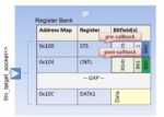
Register Modeling
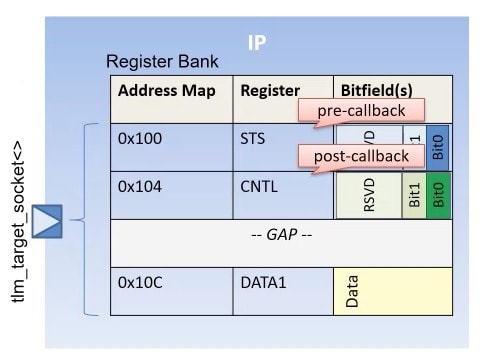
Registers provide the entry point for embedded programmers to configure an IP, and as such are universally found in almost all IPs. Registers come in all shapes and sizes and are usually described using IPXACT register specifications.
Memory mapped registers are mapped to CPU address maps. Registers may be further composed of bit-fields, each of which may control one or more aspects of an IP and report their status. Register read and write requests are typically handled via a TLM 2.0 target socket. We can marry the TLM2.0 (smart) target socket to the register library to provide seamless and automatic communication between the two.
Registers and bit-fields have five access types. The bit field read has three variants and write has ten variants. The number of permutations and combinations that this can offer is mind boggling, but with a register library, accompanied with code generation this complexity can be tucked away under a lightweight and consistent API to access registers and bit-fields. Further array-like access semantics provide syntactic sugar.
If we want to associate an action linked to a register access, we can enable it by registering a pre/post call-back with the appropriate register.
For e.g. If CNTL_BIT0 bit-field is set for an IP, then take some action. This may be implemented by providing a debug post call-back. This approach also simplifies code-reviews, as the functionality associated with a register access operation is localized, and this code can be kept separate from generated code.
static const int ADDR_CNTL = 0x104;
// Setup registers and associated bit-fields
// note: generated
void IP::register_setup() {
    // ...
}

// debug-write/post-cb (User written)
void IP::reg_cntl_cb(addr_t addr, value_t val) {
   if (m_reg[addr][CNTL_BIT0]){
       bar();
   }
}

// note: Register IP behavior
IP:IP() {
    register_setup();
    m_reg.attach_cb(ADDR_CNTL, &IP::reg_cntl_cb,
    REG_OP_DBG_WRITE, REG_CB_POST);
}
Smart TLM Sockets
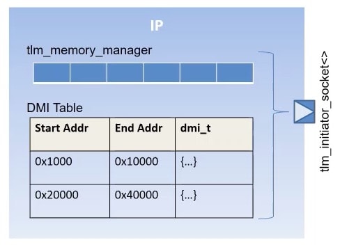
Accellera tlm_utils library provides some convenient sockets which simplify modeling TLM2.0 transactions, however they do not provide support for some commonly used features like Direct Memory Interface (DMI) management in LT modeling and tlm_mm (TLM Memory Manager) in case of AT transactions.
The TLM smart initiator socket provides built in support for tlm_mm and DMI manager that is transparent to the end-user. The tlm_mm may also be extended to support buffer, byte-enable and tlm_extensions memory management.
Similarly, TLM smart target provides a memory-mapped registration feature for resources that may be leveraged by resources like Registers and Internal Memory. It also handles gaps in memory maps based on configurable policies like ignoring them, raising an exception, etc.
Configuration
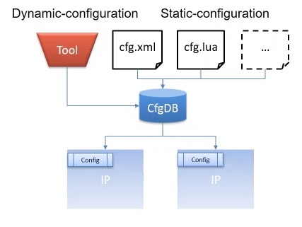
In a virtual platform you can quickly change any memory size, cache size, set policies and control debug levels using configuration. There’s a library to handle configuration aspects, and this tool reads in different file formats and then configures all of the IPs to be used in an SoC.
A configuration database provides a file-format (XML, JSON, lua etc.) agnostic way to store and retrieve configuration values, and this can be leveraged by SystemC/CCI for configuring the System.
It can support both Static (Config-file(s) based) and Dynamic (Tool based) Configuration updates. Using a Broker design pattern it can also help to limit visibility of certain parameters as desired by the IP/Integration engineer.
Reporting/Logging
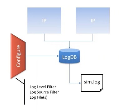
SystemC provides the hooks, albeit basic, to support reporting with log-source capture, multiple log-levels, associating actions with logging etc. What is missing is a convenience class that can simplify log management at IP and integration level, which is provided by the CST Log module..
At the IP level we need capabilities to log not just (char*) strings, but also integers, registers, internal states, etc.
At the Integration level we need capabilities to filter out messages based on the log-source(s) in addition to log-levels. For non-interactive runs, and for debugging we may want to capture logs in files.
Tool configuration is also simplified if it has access to a centralized logging module.
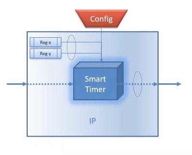
Smart Timer
It is well known that introducing clocks, especially in LT simulation can drastically slow down the simulation. While developing the models for virtual platforms, generally the clock is abstracted away, and the timing functionality is implemented in a loosely timed fashion
Every SoC have one or more timer IP, so developing the LT model of these timers can be very tedious and error prone.
CSTML has a generic ‘Smart Timer’ that can be mapped to any of your (Timer) IP needs with either Loosely Timed or Clocked styles. This class is highly configurable, and provides support for most of the commonly required timer features: using up or down counting, supporting pre-scaling, controlled with enable or pause, and having a cycle or one-shot.
Model Generator
Given an IP specification, there is a fair amount of boilerplate code needed to implement registers, internal memory, interface-handing, and configurations. Manually transcribing the specification document to code can be time consuming and introduce bugs in the process.
Using machine-readable specifications like IPXACT, custom XMLs, and Excel sheets are becoming common. The Model Generator (python based) accepts file inputs (in different formats) to describe any IP block, and then it automatically creates the boilerplate code needed for:
- IP scaffolding including interfaces, registers, any internal memories, tlm-socket to register/memory binding, configuration params
- Doxygen comments provide contextual info drawn from the Inputs.
- User-code to be written is generated in separate sources, so that the IP code can be regenerated, if required, without loss of user customizations.
- Unit testbench (UT) with complementary interfaces, sanity test cases for testing memory map, registers, configurations.
- A Top module to instantiate and connect IP and UT.
- Configuration file(s) for IP/UT and Top.
- Build scripts (Cmake based) for building and testing IP.
- README.md to provide basic information on the IP, how to build, test.
You don’t have to start with a blank screen and hand-code all of the low-level details when you use the Model Generator approach. It even creates code that conforms to your own style guidelines for consistency.
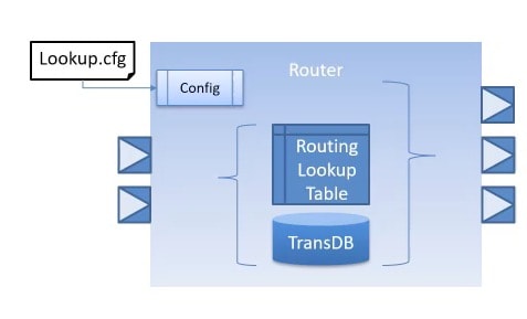
Generic Router
Once we have a set of Master and Slave IPs, the next logical step is to connect them together based on the System memory-map. This is a common IP block required in a system, and CircuitSutra has made their generic router configurable to enforce your routing policy, it’s aware of DMI, and follows your security policies. All of the options are configurable with an external file.
The generic router provides a way to configure N-initiator and M-targets. The target memory map is configurable for each initiator. It also optionally provides a way to base-adjust the outgoing transaction address. Error handling of unmapped regions can also be configured.
Alternate routing policies like round-robin, fixed-routing and priority routing can also be implemented. The router can also be made DMI aware, handing not only the normal/debug transport APIs, but also the DMI forward transport interface with base-adjustment, and invalidate DMI backward interface. The handles both LT and AT style TLM requests. Logging the configured memory maps and time stamped transactions is very helpful during debugging.
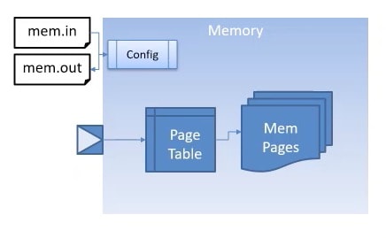
Generic Memory
Many SoC devices are filled with over 50% area of memory IP blocks. It is good to have a generic memory model that can range in size from a few MB up to multi-GB array. You configure each memory IP, define RW permissions, use logging and tracing for debug, and model single or multi-port instances.
Multiple configuration knobs are supported like the size of memory, read-write permissions and latency, byte-initialization at reset, and retention. It may also provide a feature to save/restore memory state to files. LT friendly memory implementations also provide support for DMI. Logging and tracing memory transactions are provided to help in debugging. More complex implementations may provide multiple ports with configurable arbitration policies
Python Integration
Test engineers do not have to be C++/SystemC experts to test the IP functionality. If the test scenarios are enumerated, they may be coded in any (scripting) language. A Python front-end for SystemC is quite popular due to its ease of interface with C/C++ code, and the general familiarity of engineers with the Python language. Writing tests in Python makes them more readable with fewer lines of code, and consequently fewer bugs. CSTML provides a generic testbench infrastructure that allows creating consistent self-checking unit test cases.
Summary
A well designed SystemC modeling methodology can be a big productivity boost to create a Virtual Platform more quickly with less engineering effort and shorter debug than starting from scratch. The engineers at CircuitSutra have been honing their ESL design skills over the past decade using SystemC and their libraries across a wide range of domains:
- Automotive
- Storage
- Application processors
- IoT
They are working with leading EDA, semiconductor and systems companies.
View the archived tutorial from DVCon, starting at time point 21:40.
Related Blogs


