The annual VLSI Symposium provides unique insights into R&D innovations in both circuits and technology. Indeed, the papers presented are divided into two main tracks – Circuits and Technology. In addition, the symposium offers workshops, forums, and short courses, providing a breadth of additional information.
At this year’s symposium, a compelling short course was: “Advanced Process and Device Technology Toward 2nm-CMOS and Emerging Memory”. A previous SemiWiki article from Scotten Jones gave an excellent summary of the highlights of (part of) this extensive short course. (link)
Due to space limitations, Scotten wasn’t able to delve too deeply into the upcoming introduction of Gate-All-Around (GAA) technology. This article provides a bit more info, focusing on material presented in the short course by Jin Cai from TSMC’s R&D group, entitled: “CMOS Device Technology for the Next Decade”.
FinFET to GAA Transition
Successive generations of FinFET process technology development have resulted in tighter fin pitch and taller fins, with increasingly vertical fin sidewall profile. Significant improvements in drive current per unit area have been realized. The electrostatic control of the gate input over the three surfaces of the vertical fin has also improved subthreshold leakage currents.
Yet, Jin highlighted that, “Free carrier mobility in the vertical fin is adversely impacted for very small fin thickness. TSMC has introduced SiGe (for pFETs) at the N5 node, to improve mobility. Strain engineering continues to be a crucial aspect of FinFET fabrication, as well.” (nFET: tensile strain; pFET: compressive strain)
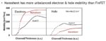
The figure below illustrates the trends in short-channel effect and carrier mobility versus fin width.
Jin continued, “An optimal process target is ~40-50nm fin height, ~6nm fin thickness, and ~15nm gate length, or 2.5X the fin thickness.”
The next step in device scaling is the horizontal gate-all-around, or “nanosheet” (NS) configuration. A superlattice of alternating Si and SiGe layers are fabricated on the wafer substrate. A unique set of etch/dep steps are used to remove the SiGe material at the NS layer edges and deposit a spacer oxide in the recessed area, leaving the Si layer sidewalls exposed. Source/drain epitaxy is then grown out from the Si sidewalls, providing both the S/D doping and structural support for the Si nanosheets. The SiGe layers in the nanosheet stack are then selectively removed, exposing the Si channels. Subsequent atomic layer deposition (ALD) steps introduce the gate oxide stack, potentially with multiple workfunctions for device Vt offerings. Another ALD step provides the gate material, fully encapsulating the nanosheet stack.
Jin focused on the carrier mobility characteristics of the nanosheet-based GAA device, as representative of performance. (More on GAA parasitic capacitance and resistance shortly.) The figure below provides an illustration of the crystalline orientation for GAA devices, to optimize the lateral mobility in the horizontal nanosheet layer channels.
Jin highlighted a key issue facing the development of NS process technology – the (unoptimized) hole mobility is significantly less than the nFET electron mobility, as illustrated below.
Digression: Carrier Mobility and Circuit Beta Ratio
When CMOS technology was first introduced, there was a considerable disparity in nFET electron and pFET hole mobility in strong inversion. A general circuit design target is to provide “balanced” RDLY and FDLY delay (and signal transition) values, especially critical for any circuit in a clock distribution network. As a result, logic circuits adopted device sizing guidelines, where Wp/Wn was inversely proportional to the carrier mobility ratio – i.e., Wp/Wn ~ mu_electron/mu_hole. For example, a device sizing “beta ratio” of ~2.5 was commonly used.
(Wp and Wn are “effective” design values – for logic circuit branches with multiple series devices, to maintain the same effective drive strength, wider devices are required.)
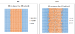
With process technology scaling employing thinner channels below the oxide surface, and with extensive channel strain engineering, the ratio between electron and hole mobility was reduced, approaching unity. Indeed, as illustrated below, the introduction of FinFET devices with quantized width values depended upon the reduction in carrier mobility difference. (Imagine trying to design logic circuits with a non-integral beta ratio in the 2+2 fin standard cell image shown below.)
Nanosheet Circuit Design
The figure above depicts a standard cell library image, for both current FinFET and upcoming nanosheet technologies. Unlike the quantized width of each fin (Wfin ~ 2*Hfin + Tfin), the nanosheet device width is a continuous design parameter, and (fortuitously) can more readily accommodate a unique beta ratio.
Note that there will be limits on the maximum nanosheet device width. The process steps for selectively removing the interleaved SiGe superlattice layers and the deposition of the oxide and gate materials need to result in highly uniform surfaces and dimensions, which will be more difficult for wider nanosheet stacks.
Speaking of nanosheet stacks, it should also be noted that the layout device width is multiplied by the number of nanosheet layers. Jin presented the results of an insightful analysis evaluating a potential range of layers, as shown below.
A larger number of layers increases the drive current, but the (distributed) contact resistance through the S/D regions to the lower layers mitigates this gain. The majority of the published research on nanosheet technology has focused on ~3-4 layers, for optimal efficiency.
Parenthetically, there has also been published research investigating nanosheet fabrication process techniques that would locally remove one (or more) nanosheet layers for a specific set of devices, before ALD of the surrounding oxide and gate. In other words, some devices could incorporate less than 3 layers. Consider the circuit applications where a weak device strength is optimum, such as a leakage node “keeper” or a pullup device in a 6-transistor SRAM bitcell. Yet, the resulting uneven surface topography adds to the process complexity – the upcoming introduction of GAA technology may not offer a variable number of nanosheet layers. The same surface topography issue would apply toward a GAA process that would attempt to build nFETs from superlattice Si layers and pFETs from superlattice SiGe layers, assuming the ability to selectively etch Si from SiGe for pFETs.
The net for designers is that GAA technology will offer (some) variability in device sizing, compared to the quantized nature of FinFETs. Leakage currents will be reduced, due to the GAA electrostatics surrounding the nanosheet channel (more on that shortly).
Analog circuits may be more readily optimized, rather than strictly relying upon a ratio of the number of fins. SRAM cell designs are no longer limited to the PD:PU:PG = 2:1:1 or 1:1:1 FinFET sizing restrictions.
Currently, FinFET standard cell libraries offer cells in integral 1X, 2X, 4X drive strength options, often with 3 or 4 device Vt variants. With greater sizing freedom (and potentially fewer device Vt alternatives) in a GAA technology, library designers have a different set of variables from which to select. It will be interesting to see how cell library designers utilize this device flexibility.
Ongoing Nanosheet Fabrication R&D
Jin described three areas of active process R&D for more optimum nanosheet characteristics.
- increased SiGe stoichiometry for pFETs
The lower hole mobility in nanosheet Si layers is a concern. Research is ongoing to increase the SiGe composition in pFET nanosheet layers (without adopting a SiGe superlattice stack, due to the topography difficulties mentioned above). One approach would be to “trim” the pFET Si nanosheet thickness after superlattice etch, and deposit a SiGe “cladding” layer, prior to oxide and gate deposition. The difficulty would be maintaining a uniform nanosheet thickness after the trim and SiGe cladding deposition steps.
- optimization of parasitic Cgs/Cgd capacitances
FinFETs have a (relatively) high parasitic capacitance between gate and source/drain nodes, due in part to the gate vertical sidewall-to-S/D node capacitance contribution between fins. The horizontal nanosheet utilizes a different gate-to-S/D oxide orientation, arising from the inner spacer deposited in the SiGe superlattice layers prior to S/D epitaxy and SiGe etch. Jin highlighted that the nanosheet and recessed oxide dimensions need to be optimized not only for the drive current, but also the parasitic Cgs/Cgd capacitances, as illustrated below.
- bottom nanosheet “mesa” leakage
The GAA topology improves upon the (3-sided) FinFET electrostatics, reducing subthreshold device leakage current. However, there is a parasitic leakage path for the very bottom (or “mesa”) nanosheet layer. After the superlattice etching, oxide dep, and gate dep steps, the gate-to-substrate electrostatics offers a (non-GAA) channel current path.
As illustrated above, Jin highlighted R&D efforts to reduce this leakage current contribution, through either:
- additional impurity introduction below the nanosheet stack
- partial dielectric isolation between the substrate and S/D nodes
- full dielectric isolation between the substrate, S/D nodes, and bottom layer nanosheet gate
Summary
Jin’s presentation offered great insights into the relative characteristics of FinFET and GAA devices, as process nodes evolve to the horizontal nanosheet topology. Designers will benefit from reduced leakage currents and design sizing flexibility, although disparities between nanosheet channel electron and hole mobility will require renewed consideration of circuit beta ratios. Ongoing process R&D efforts are seeking to reduced this carrier mobility difference, and optimize parasitic Rs, Rd, Cgs, and Cgd elements.
Jin presented a rough timeline shown below, for the introduction of GAA nanosheet technology, before new device configurations (e.g., 3D silicon fabrication) and non-silicon materials (e.g., 2D semiconductors) will emerge.
As Scotten also suggested in his article, if you have the opportunity, I would encourage you to register and view this enlightening VLSI Symposium short course.
-chipguy


