At the 2021 VLSI Technology Symposium, Imec presented on Ruthenium (Ru) and Molybdenum (Mo) as alternate Word Line (WL) materials for 3D NAND Flash “First Demonstration of Ruthenium and Molybdenum Word lines Integrated into 40nm Pitch 3D NAND Memory Devices”. I had an opportunity to interview one of the authors: Maarten Rosmeulen.
The current state of the art in NAND Flash memory is 3D NAND with ever increasing number of layers, for example at the same conference Samsung presented their forthcoming 176-layer 3D NAND process that is a follow up to their 128-layer process. One notable aspect of the Samsung announcement was that they reduced the height of their memory cells for the 176-layer process to control the height of the overall memory stack. Micron and SK Hynix have also announced 176-layer processes and Kioxia has announced a 162-layer part following their 128, 128 and 112-layer processes, respectively.
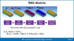
As the layer count increases, there is pressure to shrink the layer thicknesses to control the height of the stack for patterning and stress reasons as Samsung has done for their 176-layer process. The most prevalent type of 3D NAND in the industry is Charge Trap flash using a replacement metal gate (RMG) process. In the RMG process, alternating layers of oxide and nitride are deposited, the nitride is a sacrificial film that is later removed and replaced with the metal gate and a metal sheet that serves as the word line, see figure 1.
Figure 1. Replacement Metal Gate Process.
Currently the word line material of choice is Tungsten (W).
The resistance of a conductive line is given by:
R = ρL/A,
where ρ is the resistivity, L is the length and A is the cross-sectional area.
As the nitride layer thickness is reduced, the resulting replacement metal sheet is getting thinner reducing the cross-sectional area and at small dimensions ρ increases due to electron scattering further compounding the increase in resistance. Increases in word line resistivity lead to slower program/erase times for the product.
The degree to which the resistivity increases at small dimensions is partially determined by the electron mean free path in the material. The increase in resistivity at small dimensions can result in materials with relatively higher resistivity in bulk having lower resistivity at small dimensions. A figure of merit for materials at small dimensions is the bulk resistivity multiplied by the electron mean free path. Figure 2 presents some data on material resistivity.
Figure 2. Alternate Word Line Material Resistivity.
From figure 2 both Mo and Ru will have potentially lower resistivity at small dimensions than W. Of course, the values in figure 2 are just bulk values and do not necessarily translate to actual devices structures and the purpose of this work is to experimentally measure the performance.
In this work a five-layer device was created to evaluate the resistivity and transistor performance with these alternate materials. Because Imec is a research facility it is not feasible for them to create 176-layer devices, but the 5-layer device preserves the essential physics.
Figure 3 presents the resistivity of Mo and Ru for WL with thicknesses of 35nm, 25nm and 20nm. Ru shows lower resistivity than Mo in all cases studied.
Figure 3. Word Line Resistivity.
Figure 4 presents Mo transistor performance and it is better than Ru (not shown).
Figure 4. Mo Transistor Performance.
Figure 5 compares program erase for Mo and Ru and Mo shows faster program/erase than Ru.
Figure 5. Program Erase.
Finally, figure 6 compares retention for Mo and Ru, Ru is better than Mo but Mo performance is very close.
Figure 6. Retention.
Comparing the performance, Ru is better for resistivity and Mo is generally better for transistor performance.
The key question this work is trying to answer – is one of these materials a better alternative to W for thin word lines. In this work the resistivity and transistor performance of W has not yet been measured under the same conditions and this is planned for future work.
I asked whether they had a sense of when W would have to be replaced in commercial devices and he said they did not, that ultimately the specific of individual products would determine this based not only on layer thickness but ultimately on what latency the overall device achieves, this may also be application dependent.
We also briefly discussed cost, my company IC Knowledge LLC is the world leader in cost modeling of semiconductors and MEMS, and I mentioned I thought Ru was too expensive for use in 3D NAND, he said he has colleges looking at this. I did some quick calculations using our Strategic Cost and Price Model and what I see is precursor costs of around $10 to $20 per wafer for W and Mo, and Ru is over an order of magnitude more expensive in my opinion making Ru too expensive to use.
In conclusion this work is an important step towards determining the suitability of Ru and Mo as long-term replacements for W to enable continued layer scaling and improved performance.
Also Read:
VLSI Technology Symposium – Imec Forksheet
VLSI Symposium – TSMC and Imec on Advanced Process and Devices Technology Toward 2nm