– Strong demand across logic/memory & leading/trailing edge
– Customers want units fast-no time to test
– The main question is can ASML ramp to meet demand?
Revenue & Earnings low due to systems being rushed to customers
ASML reported Euro 4B in sales and Euro 1B in net income which while within guidance was on the surface low as systems were shipped prior to being tested which meant the revenue can’t be booked until they are tested at the customer site, which delays revenue recognition by a quarter.
This delayed revenue is not the real news, the real news is that customers as so desperate they want systems faster than the normal procedure.
Obviously chip customers are clamoring for capacity and ASML is trying to do their part to accommodate the situation.
ASML had expected business to be up 30% in 2021 it now looks like business will be up 35%
Orders are off the charts
Orders were Euro 8.3B with Euro 4.9B of that for EUV. This is up huge from q!’s Euro 4.7B. Memory business was up from 24% to 29% of orders. Guidance is for Q3 to be Euro 5.2B to 5.4B with gross margins of 51% to 52%.
Dry tools staging a comeback
Perhaps the best evidence of how broad based the chip shortage is, is that demand for “dry” ArF systems is growing and the company is going to unusual lengths to satisfy that unusual demand. These systems are used in older technology fabs at large line width technology certainly not anything close to leading edge.
This likely addresses autos, appliances, IOT and other mid to trailing edge technology
EUV for memory starting up
We are starting to see the early stages of EUV for memory applications. We think this could be very fortuitous timing in that memory demand could help make up for any slow down in business driven after the near term shortage and panic abates. We don’t expect this higher level of business across the board to last forever as the shortage will eventually be filled.
Having memory ramp up its need for EUV would create a very nice “backfill” of business as shortage driven business subsides. This would also be good to help fill any potential slowness created by any delays or other issues with high NA EUV.
Ramping as fast as possible
The main risk we see with ASML right now is just one of being able to ramp as quickly as demand. Lenses and other specialty components simply can’t be rushed to have capacity increase at the drop of a hat. ASML has a number of key suppliers, such as Zeiss, and there a limited number of Germans with the requisite skill sets and a limited number of the highly complex machines used to make the lenses.
As we have pointed out several times before, its a lot like trying to increase the supply of 15 year old single malt scotch. There are many time constraints.
Despite the difficulty ASML seems to be doing a very good job of expediting and prioritizing what they can. Its not so much an allocation of money as it is an allocation of resources which are more limited than money.
Right now, the lack of being able to ship to China is more of a blessing in that ASML is barely able to keep up with existing demand without more customers.
Intel likely ramping EUV
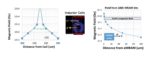
The US was only 3% of business last quarter and doubled to 6% this quarter which is still miles behind Taiwan at 36% and Korea at 39% and also trails China (non EUV) at 17%. But we would take this as a sign that Intel could be taking more EUV tools finally.
Collateral Calls
We would expect the rest of semiconductor equipment makers to report similarly strong business and orders. Perhaps not as huge as ASML but very strong upside as the demand appears very broad based and not just EUV.
Litho systems tend to lead dep and etch and others systems by a couple of quarters given lead times but in the current panic situation its highly likely that chip companies are just ordering anything that isn’t nailed down less they get stuck at the end of the line.
The Stocks
ASML trades at a very high but well deserved , monopoly like multiple. Business is not slowing any time over the next several quarters and will likely extend over a longer period than other semiconductor equipment companies due to the memory adoption of EUV which will not drive the dep and etch companies as much.
We remain concerned that the stocks are fully valued and have a hard time breaking through a somewhat plateau valuation over the last several months. Although we expect very strong earnings and orders from all semiconductor equipment companies we don’t know if we will see a corresponding increase in stock values.
About Semiconductor Advisors LLC
Semiconductor Advisors is an RIA (a Registered Investment Advisor),
specializing in technology companies with particular emphasis on semiconductor and semiconductor equipment companies. We have been covering the space longer and been involved with more transactions than any other financial professional in the space. We provide research, consulting and advisory services on strategic and financial matters to both industry participants as well as investors. We offer expert, intelligent, balanced research and advice. Our opinions are very direct and honest and offer an unbiased view as compared to other sources.
Also Read:
GloFo inside Intel? Foundry Foothold and Fixerupper- Good Synergies
Chips for America Act – Funding Failures & Foreigners or Saving Semiconductors?