-Chips for America is better than nothing, but not much
–TSMC $40-44B Capex crushes competition (Intel & Samsung)
-Additional efforts other than handouts are necessary
-Could/should TSMC be “adopted” as a US company?
Competition can’t keep up with $40-$44B of Capex
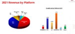
TSMC’s recent announcement of $40-$44B of capex spending is a mind blowing number that is a large increase from last years huge number and makes them far and away the biggest spender period.
Both Intel and Samsung can’t hope to spend anywhere near that number.
If we assume some is for expansion of existing non leading edge capacity but the majority is aimed at the leading edge it means a dominant share of capacity and a very dominant share of EUV and other advanced enabling tool sets.
$52B Chips for America is barely a rounding error
When you assume that the Chips for America act is a one time, one shot disbursement spread over a number of years and a number of companies it becomes clear that its not much against TSMC’s spend.
It also does not compare to what China as a whole is spending on semiconductor technology.
Basically the US is being outclassed and outgunned by both China and Taiwan ( probably part of China in the not too distant future).
Even if Intel got the whole $52B it still couldn’t keep up as the spend would be over several years. Never mind that only $10B of the $52B is for fab projects with a $3B limit per project. Essentially the $52B will be spread so thin as to be ineffective versus the focused sharp spend of TSMC.
Can the US fabs being built make a difference?
Intel announced two fabs in Arizona at $10B each along with TSMC announcing a 5NM fab in Arizona which by the time its operational will be a drop in the bucket trailing edge fab perhaps meant to mollify the US.
Samsung has announced a $17B in Texas in addition to existing facilities there.
It looks like Intel has chosen Ohio for its “megafab” project and Micron is eyeing North Carolina.
While details are scarce, it sounds like the Intel Ohio and Samsung Texas fabs are the most impactful on the US. Samsung would be somewhat less impactful as we assume that bleeding edge technology R&D will continue to be done in Korea making the Texas fab a “fast follower” much as the existing Samsung fab in Texas is today. That leaves Intel Ohio as the only trail blazing R&D facility in the US.
It also remains to be seen if the brain trust in Portland can either be moved or shared with Ohio or if Portland remains the R&D center with Ohio for production.
Excellent CNET article
All this begs the question as to why we can’t get TSMC in the US?
(In a real way)
Obviously TSMC’s brain trust is in Taiwan but could it be both re-created and/or moved to some extent with the right incentives? Rather than a token trailing edge fab in the US, a real leading edge state of the art complete with R&D?
Maybe grant citizenship to those employees willing to move to escape a potential China take over or at least hedge against it.
Throw a lot of money at them, along with a nice life in the US.
It might be a much more reliable and expedient way of fixing the US’s chip problem as compared to trying to rebuild Intel or take hand me downs from Samsung.
Right now time is not on the US’s side and we need chip capacity and expertise fast. We cannot wait ten years for Intel to build a fab and get critical employee mass in Ohio starting with a literal greenfield.
We need to think outside the box or get left behind
Incentives and disincentives are needed in addition to Chips for America
The cost of a semiconductor fab is similar around the world as the majority is the cost of the equipment which costs the same wherever you are (or should it?)
Could/should the US put export taxes on US semiconductor equipment (whether made in the US or a foreign subsidiary but with US technology)
Maybe a 50% tax on tools going to China, maybe 25% on Taiwan. Penalize those companies who would try to trans ship equipment to China. Use the received funds to support the US chip industry.
Incentivize all the companies, Intel, Micron, TSMC and others to build fabs in the US because the primary cost, equipment, would be cheaper here.
We could also go back to prior export restrictions that limited US tool exports to equipment that was several generations old. This technology export restriction worked well with SMIC and China for years but was removed over the years as relations improved (even though relations are now souring again).
The US seems to forget that the majority of semiconductor tools have their basis in US technology (including EUV made by ASML).
Is it better to throw money at the problem as compared to controlling our own fate through our own technology?
Where are the non-handout protections and incentives in the Chips for America act?
In a zero sum game equipment makers don’t get hurt, consumers pay a little more for US made…
As the world needs a certain amount of semiconductors and it takes a certain amount of equipment to make them. Equipment makers would sell the same amount of equipment just to different end locations.
Any chip maker, foreign owned or US owned would benefit by having a fab in the US.
End consumers would likely have to pay a little more for chips made in the US rather than China , but I would rather pay a little more and be able to buy a car and a computer when I need one and not held hostage.
Removing an attractive target- “Broken Nest”
From a political and global strategic perspective it is the existence of TSMC in Taiwan that likely creates additional instability in the region vis a vis China. If Taiwan were a backward Island of farmers China would not be so focused on getting hold of it and would likely not be doing as much saber rattling.
It is the mere fact that Taiwan contains exactly what China desperately needs right now, semiconductor dominance, that makes it such an attractive target, worthy of a lot of effort and bloodshed to obtain.
Remove semiconductors from Taiwan and suddenly the target’s value is greatly diminished and maybe not worth starting a war over.
This is not unlike the middle east and its supply of oil that made it so strategically important. If it were just a desert with camels, no one would care.
Could Taiwan be less attractive if China wasn’t getting TSMC? Could that cool the current tensions?
Broken Nest: Deterring China from invading Taiwan
The stocks
The stocks have lost a little steam as the rapid run up has lost some momentum with less new news and concerns about some sort of peak.
The TSMC capex news underscores that 2022 will continue to be a very good year for chips and likely better than 2021.
Although there is the possibility of slowing, it appears that current momentum remains strong enough to make it a very good year.
We remain most positive on the arms merchants…the semiconductor equipment stocks as its clear that “wartime” spend in the chip industry continues to increase benefitting the tool makers.
While TSMC stands to make a huge amount of money from the continued supply demand imbalance it seems to be plowing most of that money back into capex so its unclear exactly how much will result in increased profitability.
This is even more so the case with Intel that has more spending projects than they currently have money for. First Intel has to figure out where the money is coming from. It looks as if they have already committed their entire market cap in spend over all the projects they have announced.
Even if the Chips for America act is a “gift” to Intel, they are still billions short of what they need.
Samsung will not be left out and will likely double down as well.
The main risk we see, at least in the near term remains supply chain issues limiting tool makers and other kinks in the supply chain like fires in Berlin and new variations of Covid locking down China again.
The usually seasonally weak Q1 is not
Perhaps one of the best signs we see is that usually Q1 is the weakest quarter of the year for chips as we are in a post partum depression after the selling frenzy of the holiday season coupled with a couple of weeks for Chinese new year. Q1 is also usually the low point for memory pricing again related to slower demand.
We are not seeing as much of the normal “seasonal” slowing in the industry. Demand for chips seems undaunted. We had previously thought that we would start to see an easing of the crunch in 1H of 2022 but it seems to be longer lasting.
We still question how long it lasts as the industry remains a cyclical one by its very nature but demand remains overwhelming for the time being.
We may see some psychological weakness as investors are concerned about a cyclical peak or Covid news. Even though business increases may be as good as 2021, we don’t think the stocks will move quite as quickly as they did last year and may prove more volatile on the way.
For now, memory seems stable, but that is usually the first thing to fall. Memory makers seem to be maintaining a rational spend and technology pattern that continues to support profitability. If anything , Micron is probably more undervalued given the current circumstance.
Chip equipment companies need to be razor focused on execution as the demand is there if they can make product.
Also Read:
“Too Big To Fail Two” – Could chip failure take down tech & entire economy?
Semicon West is Semicon Less
Supply Chain Breaks Under Strain Causes Miss, Weak Guide, Repairs Needed


