Lauro Rizzatti recently interviewed Jean-Marie Brunet, vice president of product management and product engineering in the Scalable Verification Solution division at Siemens EDA, about why hardware-assisted verification is a must have for today’s semiconductor designs. A condensed version of their discussion is below.
LR: There were a number of hardware-assisted verification announcements in 2021. What is your take on these announcements?
JMB: Yes, 2021 was a year of major announcements in the hardware-assisted verification space.
Cadence announced a combination of emulation and prototyping focused on reducing the cost of verification by having prototyping take over tasks from the emulator when faster speed is needed.
Synopsys announced ZeBu-EP1, positioned as a fast-prototyping solution. It isn’t clear what the acronym means, but I believe it stands for enterprise prototyping. After several years of maintaining that ZeBu is the fastest emulator on the market, Synopsys launched a new hardware platform as a fast (or faster) emulator. Is it because ZeBu 4 is not fast enough? More to the point, what is the difference between ZeBu and HAPS?
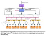
In March 2021, Siemens EDA announced three new Veloce hardware platform products: Veloce Strato+, Veloce Primo and Veloce proFPGA. Each of these products addresses different verification tasks at different stages in the verification cycle. The launch answered a need for hardware-assisted verification to be a staged, progressive path toward working silicon. Customers want to verify their designs at each stage within the context of real workloads where time to results is as fast as possible without compromising the quality of testing.
In stage 1, blocks, IP and subsystems are assembled into a final SoC. At this stage, very fast compile and effective debug is needed with less emphasis on runtime.
At stage 2, the assembled SoC is becoming a full RTL description. Now, design verification requires a hardware platform that can run faster than the traditional emulator. One that needs less compilation, less debug but more runtime.
In stage 3, verification moves progressively toward system validation. Here it’s about full performance where cabling interconnect to the hardware allows it to run as fast as possible.
LR: Let’s look at the question of tool capacity. Some SoC designs exceed 10-billion gates making capacity a critical parameter for hardware platforms. A perplexing question has to do with capacity scalability. For example, does a complex, 10-billion gate design (one design) have the same requirements as 10, one-billion gate designs (multiple designs) in terms of usable emulation capacity?
JMB: This question always triggers intense discussions with our customers in the emulation and prototyping community. Let me try to explain why it’s so important. Depending on the customer, their total capacity needs may be 10-, 20- or 30-billion gates. In our conversation with customers, we then inquire about the largest design they plan to emulate. The answer depends on the platform they’re using. Today, the largest monolithic designs are in the range of 10- to 15-billion gates. For the sake of this conversation, let’s use 10-billion gates as a typical measure.
The question is, do they manage a single monolithic design of 10-billion gates in the same way they manage 10, one-billion gate designs? The two scenarios have equivalent capacity requirements, but not the same emulation complexity.
Emulating a 10-billion gate design is a complex task. The emulator must be architected to accommodate large designs from the ground up through the chip and subsystem to the system level including requirements at the software level.
A compiler that can map large designs across multiple chips, across multiple chassis is necessary. A critical issue is the architecture that drives the emulation interconnect. If not properly designed and optimized, overall performance and capacity scaling drops considerably.
With off-the-shelf FPGAs as the functioning chip on the boards, the DUT is spread across each interconnected FPGA, lowering the capacity of each FPGA. By interconnecting multiple chassis, the overall performance drops below that of one or a few FPGAs.
Synopsys positions its FPGA-based tools as the fastest emulator for designs in the ballpark of one-billion gates. The speed of the system clock is high because FPGAs are fast. When enough hardware is assembled to run 10-billion gates, an engineer ends up interconnecting large arrays of FPGAs that were never designed for this application. And typically, the interconnection network is an afterthought conceived to accommodate those arrays. This is different from a custom chip-based platform where the interconnection is designed as an integral part of the emulator.
Cadence claims support for very high capacity in the 19-billion gate range. The reality is that no customer is emulating that size of design. The key to supporting high-capacity requirements is the interconnect network. It doesn’t appear that the Palladium Z2 interconnect network is different from the network in Palladium Z1, which is known for capacity scaling issues. As a result, customers should ask if Palladium Z2 has the ability to map a 10-billion gate design reliably.
Today, Veloce Strato+ is the only hardware platform that can execute 10-billion gate designs in a monolithic structure reliably with repeatable results without suffering speed degradation.
The challenge concerns the scaling of the interconnect network. Some emulation architectures are better than others. Based on the roadmap taken by different vendors, future scaling will get even more challenging.
By 2025, the largest design sizes will be in the range of 25-billion gates or even more. If today’s engineering groups are struggling to emulate a design at 10-billion gates, how will they emulate 25 billion+ gates?
Siemens EDA is uniquely positioned to handle very large designs, reliably and at speed, and we continue to develop next-generation hardware platforms to stay ahead of the growing complexity and size of tomorrow’s designs.
LR: Besides the necessary capacity, what other attributes are required to efficiently verify complex, 10-billion gate designs?
JMB: Virtualization of the test environment is as important as capacity and performance.
In the course of the verification cycle, the DUT representation evolves from a virtual description (high level of abstraction) to a hybrid description that mixes RTL and virtual models, such as AFMs or QEMU. Eventually, it becomes a gate-level netlist. When an engineer is not testing a DUT in ICE (in circuit emulation) mode, the test environment is described at a high level of abstraction typically consisting of software workloads.
It’s been understood for a while that RTL simulation cannot keep up with execution of high-level abstraction models running on the server. The larger the high-level abstraction portion of the DUT, the faster the verification. The sooner software workloads are executed, the faster the verification cycle. This is the definition of a shift-left methodology. A virtual/hybrid/RTL representation is needed to run real software workloads on an SoC as accurately as possible and as fast as possible. An efficient verification environment allows a fast, seamless move from virtual to hybrid, from hybrid to RTL, and from RTL to gate.
The hybrid environment decouples an engineer from the performance bottleneck of full RTL, which supports much faster execution. In fact, hybrid can also support software development that is not possible in an RTL environment. A full RTL DUT runs in the emulator with very limited interaction with the server in hybrid mode or the parts of the DUT that run on the server. Here the connection between server and platform, or what we call co-model communication, becomes critical. If not architected properly, the overall performance fails to be acceptable. Unlike the bottleneck of the emulator, now the bottleneck is the communication channel.
We have invested significant engineering resources to address this bottleneck. Our environment excels in virtual/hybrid mode because of our unique co-model channel technology
Capacity, performance and virtualization are the key attributes to handle designs of 10+-billion gates. When designs hit 25 billion+ gates in 2025, the communication channel efficiency becomes even more critical since hybrid emulation becomes prevalent in a wide range of applications.
LR: Thank you, Jean-Marie, for your perspectives and for explaining some of the little-known aspects of successful hardware emulation use.
Also Read:
DAC 2021 – Taming Process Variability in Semiconductor IP
DAC 2021 – Siemens EDA talks about using the Cloud
DAC 2021 – Joe Sawicki explains Digitalization


