
IBM transferred their semiconductor manufacturing to GLOBALFOUNDRIES several years ago but still maintains a multibillion-dollar research facility at Albany Nanotech. IBM is very active at conferences such as IEDM and appears to have a good public relations department because they get a lot of press.
At the Litho Workshop in 2019 I heard an IBM presentation from the Albany research group, explaining that IBM had to have the research line because they needed state-of-the-art technology for the processors that run their computers. I personally question this rational, the Albany Research group collaborated with Samsung on the 5nm process Samsung put into production. I estimate that Samsung’s 5nm process when compared to TSMC’s 5nm process – has 1.69x the power consumption (worse), 0.64x the performance (worse), and 0.72x the density (worse). I am sure there are special features in the process to support IBM, but I am also sure the same features could be implemented in the TSMC process without a multibillion-dollar research investment. I also thought it was interesting that they said that while developing the process they turned up the EUV dose until they got good yield and then they transferred it to Samsung expecting Samsung to reduce the EUV dose. When Samsung began ramping their 5nm process there were industry rumors Samsung couldn’t get enough wafers through their EUV tools (high EUV dose leads to low throughput) and the yields were low.
IBM also makes a big splash in the mainstream press every few years with some new development but in my opinion a lot of the developments don’t live up to the hype. For example, in early 2021 IBM announced the development of a 2nm technology but as I have previously written it is more like TSMC’s 3nm process that 2nm, and unlikely to be competitive versus expected 2nm processes from Intel and TSMC. You can read my 2nm article here: https://semiwiki.com/semiconductor-services/ic-knowledge/298875-is-ibms-2nm-announcement-actually-a-2nm-node/
This is not to say that IBM doesn’t do important research, years ago they were responsible for many key industry innovations including copper metallization, I just question whether a multibillion-dollar semiconductor research facility makes sense for a company that doesn’t make semiconductors.
In this article I will discuss three IBM papers from IEDM.
Vertical-Transport Nanosheet Technology for CMOS Scaling beyond Lateral-Transport Devices
In my opinion this paper is another example of an IBM announcement I don’t expect to live up to the hype. Authors note, this work was done in cooperation with Samsung. The mainstream media has already published about this “breakthrough” as if it will be a production solution.
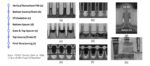
Figure 1 illustrates the Vertical-Transport Nanosheet (VTFET) process.
Figure 1. Vertical-Transport Nanosheet (VTFET) process.
The basic idea here is to make nanosheets but rather than in the horizontal direction, to turn them into the vertical direction. In the paper a vertical nanosheet is compared to a FinFET and shown to offer better performance and area. I see two issues with this.
First, my understanding is vertical transistors are very favorable for SRAM usage where the interconnect needs are simple and regular but doesn’t work well for random logic designs with complex interconnect needs. Imec has previously shown some very interesting vertical SRAM work although it doesn’t appear to have gained any traction in the industry. With the advent of chiplets a simple SRAM process that offers superior density makes a lot of sense. But once again, for logic use the vertical transistor area would likely go up a lot to accommodate the interconnect requirements.
The second issue I see with this is it is being compared to FinFETs. The transitions away from FinFETs to stacked horizontal nanosheets (HNS) is already under way. HNS offers density and performance advantages over FinFETs, but even more importantly offers a long-term scaling path. HNS can improve performance by stacking more sheets vertically, they also open the opportunity to introduce a dielectric wall creating an Imec innovation called Forksheets with reduced n to p spacing. Beyond this, stacking n and p HNS in a 3D-CMOS/CFET architecture offers more scaling with zero horizontal n to p spacing. Beyond HNS, the sheets can potentially be replaced with 2D materials providing even more scaling. Drive current and therefore performance of vertical fins is driven by the fin size, and I don’t see how the devices can scale the way HNS can. I believe this is why the industry has chosen HNS as the successor to FinFETs, Samsung is already trying to ramp a HNS process (Samsung calls it Multibridge), Intel is planning HNS (Intel calls them RibbonFETs) for 2024 and TSMC has published HNS work and is widely expected to adopt them for 2nm (although they haven’t formally announced their 2nm process technology selection).
Critical Elements for Next Generation High Performance Computing Nanosheet Technology
In my view this paper is a lot more interesting than the previous one because it is addressing issues with the HNS technology that all the major leading edge logic suppliers are facing. IBM has done a lot of good work on HNS in the past and this paper builds on that.
There are two HNS issues addressed in this paper.
The first issue is that pFET mobility is poor for HNS. IBM has previously described two techniques to improve pFET mobility, one is to trim back the channel after release and deposit a SiGe cladding layer. Another technique is fabricating the channels on a strain relaxed buffer layer.
In this paper SiGe channels were formed by depositing lower Ge content channels over higher Ge content sacrificial layers when the original nanosheet stack is deposited. The difference in Ge content is to enable the selective release etch, to etch out the sacrificial films and leave the channels intact. The SiGe channel provides improved mobility, improved performance, and greater reliability.
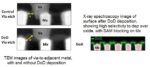
Figure 2 illustrates the SiGe channel HNS pFET.
Figure 2. SiGe channel HNS pFET.
The second issue addressed here is how to achieve multiple-uniform threshold voltages (Vts) for HNS. For FinFETs the fin-to-fin distance is relatively wide and multiple Vts can be achieved by depositing and selectively removing multiple work function metals. With HNS the sheet to sheet (Tsus) spacing is so small that there isn’t enough space for a full stack of work function metals. The metals also tend to be thicker on the outside of the NS and thinner in between the nano sheets leading to non-uniform Vts.
IBM pioneered the use of dipoles to control VT over decade ago and that technique is now getting a lot of attention for HNS because dipoles can be created by doping the high-k dielectric and don’t require extra thickness the way multiple work function metals do. Dipoles can also fix the Vt non uniformity issue.
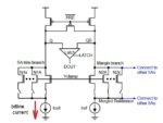
Figure 3 illustrates how work function metals can lead to non-uniform Vts and how volumeless dipoles fix the problem.
Figure 3. Work Function metal versus Dipoles for Vt control. (a) Pure metal multi-Vt scheme which could cause huge Vt non-uniformity for high nVt device and high pVt device and (b) Volumeless multi-Vt reduces nWFM thickness and share the metals to improve the Vt uniformity.
Gate-Last I/O Transistors based on Stacked Gate-All-Around Nanosheet Architecture for Advanced Logic Technologies
The third paper I wanted to discuss is another paper looking at HNS issues.
Another challenge in HNS implementation is how to create I/O transistors that can operate at higher voltage. In this paper a gate last process flow creates two different gate oxide thicknesses with a combination of deposited oxide and novel selective oxidation. The selective oxidation creates thick and thin selective oxides that are added to the deposited oxide. The key to this technique is that grown oxide consumes silicon during oxidation and therefore the thicker grown oxide consumes more silicon than the thin grown oxide opening up the sheet to sheet spacing (Tsus) to accommodate the thicker oxide.
Figure 4 illustrates thick and thin gated oxide HNS devices and the improved Tsus to accommodate the thick oxide.
Figure 4.- Thick and thin gate oxide HNS devices with increased Tsus for the thick I/O oxide devices.
Conclusion
Despite the mainstream media hype about IBM’s Vertical-Transport Nanosheet announcement at IEDM, we believe it is IBM’s work on perfecting HNS processes is more likely to have an impact on the industry. pFET channel mobility, volume less Vt solutions and high voltage I/O solutions address problems the industry is currently wrestling with for the FinFET to HNS transition


