
Predictions and trends create the forces that accelerate innovations and keep the industry moving forward. We are all used to hearing of important issues and challenges, usually in the context of solutions offered by various vendors. The SemiWiki forum plays its role in bringing awareness of all of the above to its audience. For example, many companies make presentations on a regular basis about design related challenges and solutions and SemiWiki covers many of those. But a recent webinar by the Methodics division of Perforce is different. It is different because it presented key insights gathered from a broad cross-section of the industry.
The webinar titled “Future of Semiconductor Design: 2022 Predictions and Trends” was presented by Robin Butler, General Manager of Methodics at Perforce. Robin reported the top issues, trends, challenges and solutions as learned from a survey of the industry. The key to a great survey depends on how well the industry was represented in it. The following is the breakdown of the representation.
Roles: Engineering Management (32%), Design Engineering (34%), CAD Management (13%), IT Management (1%), Executive Management (10%) and others such as Functional Safety Managers.
Experience level: from 0-2 years (13%), 3-5 years (10%), 6-10 years (14%), and 11 years or more (62%).
Companies: under $500 million annual revenue (44%), $501 million to $5 billion (26%), and over $5 billion (30%).
No matter what role one is playing within the semiconductor ecosystem, you are likely to find the results of the survey interesting. (a) Inspiration to enhance an existing product, build a new product to bridge a gap, ride a trend or solve an important issue. (b) Adoption of best design practices and asset management tools and techniques.
This post is a synthesis of the salient points I garnered from the webinar.
Most Important Issues
The two most important issues companies are facing are time-to-market pressures and effective reuse of IP. While reuse of IP is an effective way to accelerate time to market, companies need to implement formal IP reuse strategies. Lack of such formal reuse strategies, processes and supporting tools are impeding the growth in semiconductor design productivity. This is compounded by the fact that semiconductor design capacity is increasing at a rapid rate. According to a recent study by the University of Michigan, semiconductor design productivity is increasing at a rate of 28% annually. But semiconductor capacity is increasing even faster, at 58% annually.
A formal IP reuse strategy is becoming a must to deliver on time-to-market demands and close that gap between design capacity and design productivity.
Trends
Companies are increasingly required to meet ISO 26262, ITAR, and other compliance/functional safety standards. This is understandable given that many of the markets driving semiconductor growth are for consumer-oriented applications. A design and implementation tools suite that can enable, automate and ensure traceability for semiconductor design is becoming critical.
The global embedded system market is expected to grow 6.3% to $137.31 billion by 2027. Embedded software is becoming part and parcel of many of today’s products requiring hardware and software to be bundled together. As hardware designers and software developers collaborate to create the product offering, configuration management is essential to handle the interdependencies.
A majority of the survey respondents stated that 40+% of a die in a typical chip is made of custom circuitry. And analog component reuse is becoming more common to expedite design of complex mixed-signal SoCs. In other words, more analog is getting integrated into SoCs.
A significant portion of survey respondents indicated that more than half of their job requires IP integration. A comprehensive IP lifecycle management platform would make the IP integration job easier by helping find, qualify and integrate the optimal IP for the job.
What a difference a year or two makes. Implementation of 2.5D designs is trending upward. A little more than a third of the survey respondents are considering or already implementing 2.5D designs for their products. 2.5D designs are becoming more feasible and a way to maintain the level of SoC integration as Moore’s law is slowing.
Challenges
Finding relevant IPs for reuse is a challenge. Many survey respondents are either reusing IP from a previous project or asking a coworker for recommendations. While this approach works, this may or may not yield the optimal IP for the project on hand. A more formal, data-driven approach to finding relevant IP would increase design productivity and deliver a better product.
Survey respondents stated that finding relevant IP for their design takes at least a day or longer. They then need to qualify the IP for inclusion into their design. Nearly 75% of survey respondents reported difficulty in determining the context of an IP and its quality. Tracking and determining the quality of Ips is important for traceability.
An efficient way of cataloging IP using metadata from various qualification tools within the design ecosystem is an area of opportunity. A platform that can determine if requirements are met and where an IP is used can provide teams with the quality metric and state of the IP.
Tools
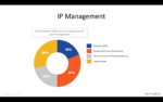
IP Management
Although companies have embraced IP-centric design practices, using a commercial IP Lifecycle platform is still in the early stages of adoption. As you can see from the Figure below, 81% of the survey respondents are not using a commercial IP Lifecyle Management (IPLM) platform. While 19% stated they are using Methodics IPLM, 28% said they use internal/other. The 28% could contain other commercial IPLM platforms. This is due to the fact that the survey was promoted in the Perforce customer base.
From an opportunity perspective for IPLM platform vendors, there is an opportunity with at least 53% of the pie below.
Data Management and Version Control
Data management and version control solutions come from the development space and for Perforce, it goes back to its early days as a company. These solutions provide a backbone for IP management. It can support the tracking of IPs and provide the metadata engineers need to make informed decisions. 36% of respondents indicated they are using Perforce Helix Core for data management, followed by 17% using Subversion (SVN) and another 17% using Git.
From an opportunity perspective for data management/version control tools vendors, there is an opportunity with at least 16%% of the pie below.
Summary
A formal IP reuse strategy is essential to make the most of one’s IP investments. It is a must to deliver on time-to-market demands and close that gap between design capacity and design productivity. With an increasing requirement for semiconductor products to meet compliance and/or functional safety standards, traceability represents a major challenge. An effective IP management platform helps designers locate, qualify and manage the release of IP. Using such a platform to manage the IP enables reuse across projects and also enables traceability.
The survey indicates that there is opportunity to maximize the potential of an IP-centric design approach with the use of the right management tools. And there is opportunity for tools vendors to tap into the prospective market potential for these tools.
To watch a recording of the webinar, click here.
The detailed results of the survey are included in a Perforce report titled “Semiconductor Report – The State of the Industry.” To get a copy of the report, click here.
Also read:
Webinar – SoC Planning for a Modern, Component-Based Approach
You Get What You Measure – How to Design Impossible SoCs with Perforce


