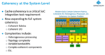
Semiwiki EDA Webinar 800x100

Demand for High Speed Drives 200G Modulation Standards

Demand for High Speed Drives 200G Modulation Standards
by Tom Simon on 01-03-2022 at 10:00 am

200G Modulation

Right now, the most prevalent generation of Ethernet for data centers is 400 Gbps, with the shift to 800 Gbps coming rapidly. It is expected that by 2025 there will be 25 million units of 800 Gbps shipped. Line speeds of 100G are used predominantly for 400 Gbps Ethernet – requiring 4 lanes each. Initially 800 Gbps will simply move to 8 lanes, but the bulk of 800 Gbps will ultimately use 200G lanes. This move to 800 Gbps and the expected use of 200G lanes is adding huge impetus to the development of modulation standards for 200G lanes.

For long reach connections line loss and power are major factors in determining what modulation method should be used in going to 200G. 100G uses 4-PAM. There is a recent video and white paper from Alphawave IP, a developer of advanced communications IP, on this topic that compares the various options. The video, titled “Connecting the Digital World—The Path to 224 Gbps Serial Links” also looks at other methods that can be used to improve data rates while not consuming excessive power. In the video Alphawave IP  President and CEO Tony Pialis reviews the options that the industry has for moving forward on 200G standards.

Tony goes through 2-PAM, 4-PAM, 6-PAM, 8-PAM, QPSK and 16-QAM comparing the tradeoffs for each. It seems that for each one there is a penalty in power, SNR or Eb/No to maintain the needed bit error rate. Doubling the frequency for 4-PAM requires more power than 6-PAM and requires more bandwidth. 2-PAM requires even more power. 6-PAM and 8-PAM suffer from decreased SNR due to the smaller constellation spacing. QPSK and 16-QAM require more channel capacity compared to PAM modulation techniques. They also suffer from increased Eb/No or power. There is more to this and I suggest viewing the video to get the full picture.

200G Modulation

Other novel methods can be utilized to help reduce errors and increase line efficiency. Tony starts by describing an advanced DSP technique that can improve the integrity of the received signal with virtually no penalty. He proposes the use of Decision Feedback Equalizers (DFE) to remove inter-symbols interference (ISI). With the receipt of each identified symbol, the remnant of that symbol can be factored out of the subsequent symbol by using DSP techniques. This makes it easier to interpret the incoming symbol.

Another application of advanced DSP techniques is Maximum Likelihood Sequence Detectors (MLSD) which creates a usable analog model of the channel to predict what various incoming symbol sequences would look like after transiting the channel. By comparing the actual received signal with various possible data patterns, the data pattern with the lowest mean square error compared to the actual signal can help identify the correct sent data.

Amplifying a signal boosts the noise just as much as the data, so smarter methods like the two listed above have a lot to offer as data rates push harder against the absolutes limits of Ethernet connections and board/package losses at higher data rates. The methods above are also very power efficient.

Tony closes with his thoughts on the use of error correction and modulation methods. 4-PAM is really not able to support longer channels. This leaves 6-PAM as a good alternative for long range links. He even hints at a standard that could mix modulation methods based on the channel. There is no doubt that the push to 200G lanes is on, and we can expect to see its use in 800 GbpE and even 1.6TbE. The full video is available here on the Alphawave IP website.

Also Read:

The Path to 200 Gbps Serial Links

Enabling Next Generation Silicon In Package Products

Alphawave IP is Enabling 224Gbps Serial Links with DSP


Advanced 2.5D/3D Packaging Roadmap

Advanced 2.5D/3D Packaging Roadmap
by Tom Dillinger on 01-03-2022 at 6:00 am

SoIC futures

Frequent SemiWiki readers are no doubt familiar with the advances in packaging technology introduced over the past decade.  At the recent International Electron Devices Meeting (IEDM) in San Francisco, TSMC gave an insightful presentation sharing their vision for packaging roadmap goals and challenges, to address the growing demand for greater die integration, improved performance, and higher interconnect bandwidth.[1]  This article summarizes the highlights of the presentation.

Background

2.5D packaging

2.5D packages enable multiple die to be laterally positioned in close proximity, with signal redistribution interconnect layers (RDL) between the die fabricated on a silicon interposer present between the die and package substrate.  Through silicon vias (TSVs) provide the connectivity to the substrate.

The TSMC implementation of this technology is denoted as Chip-on-Wafer-on-Substrate (CoWoS), as was introduced a decade ago using multiple FPGA die in the package to expand the effective gate count.

The emergence of high bandwidth memory (HBM) stacked die as a constituent of the 2.5D integration offered system architects with new alternatives for the memory hierarchy and processor-to-memory bandwidth.

The development investment in 2.5D technology grew, now enabling the silicon interposer area to greatly exceed the “1X maximum” reticle size, to accommodate more (and more diverse) processing, memory and I/O die components (aka, “chiplets”).

Additional package fabrication steps incorporate local “trench capacitors” into the interposer.  Oxide-poly-oxide-poly material layers fill the trench, with the poly connected to the RDL supply metal.  The resulting decoupling capacitance reduces power supply droop considerably.

Alternative technologies have also been developed, replacing the full area silicon interposer with a local “silicon bridge” (CoWoS-L) between adjacent die embedded in an organic interposer, thus reducing cost (albeit with relaxed RDL interconnect dimensions).

Concurrently, for very low cost applications, the demand for higher I/O count die than could be supported with the conventional wafer-level chip-scale package (WLCSP) led to the development of a novel technology that expands the die surface area with a “reconstituted wafer”, on which the redistribution to a larger number of I/O bumps could be fabricated.

This Integrated FanOut (InFO) technology was originally developed for single die (as a WLCSP-like offering).  Yet, the application of this technique is readily extended to support the 2.5D integration of multiple heterogeneous die placed adjacent, prior to the reconstitution step. (The InFO_oS technology will be discussed shortly.)

3D die stacking

3D die stacking technology has also evolved rapidly.  As mentioned above, the fabrication of TSVs spanning between layers of DRAM memory die with “microbumps” attached at the other end of the TSV has enabled impressive levels of vertical stacking – e.g., eight memory die plus a base logic controller die in an HBM2e configuration.

Similarly, through-InFO vias (located outside the base die in the reconstituted wafer material) has enabled additional micro-bumped die to be vertically stacked above the base InFO die – e.g., a memory die on top of a logic die.

The most recent advancement in 3D stacking technology has been to employ bump-less “direct bonding” between two die surfaces.  Applying a unique thermal + compression process, two die surfaces are joined.  The metal pad areas on the different die expand to form an electrical connection, while the abutting dielectric surfaces on the two die are bonded.  Both face-to-face (F2F) and face-to-back (F2B) die orientations are supported.  The planarity and uniformity (warpage) requirements of the surfaces are demanding; particulates present on the surface are especially problematic.  TSMC denotes their 3D package technology as System-on-Integrated Chips, or “SoIC”.

As product architects are exploring the opportunities available with these packaging technologies, there is growing interest in combining “front-end” 3D stacked SoIC configurations with 2.5D “back-end” (InFO or CoWoS) RDL patterning and assembly.  The collective brand that TSMC has given to their entire suite of advanced packaging offerings is “3D Fabric”, as illustrated below.

TSMC 3D Fabric Roadmap

At IEDM, TSMC shared their strategy for improving performance, power efficiency, signal bandwidth, and heat dissipation for these technologies.  (The majority of the focus was on bonding technology for SoIC.)

CoWoS (2.5D)

    • increase package dimensions to 3X maximum reticle size for the Si interposer
    • expectation is that stacked SoIC die will be integrated with multiple HBM stacks

InFO_oS (2.5D)

The original InFO offering was as an evolution to WLCSP, first as a single die, and then as a base die with another added on top connected to the through-InFO vias.  TSMC is also expanding the InFO offering to support multiple adjacent die embedded in the reconstituted wafer; the RDL layers are then fabricated and microbumps added for attach to a substrate (InFO-on-Substrate, of InFO_oS).  A projection for the InFO_oS configurations to be supported is illustrated below.

SoIC (3D)

The roadmap for 3D package development is shown below, followed by a table illustrating the key technical focus – i.e., scaling the bond pitch of the (F2F or F2B) stacked connections.

The bond pitch (and other metrics) for microbump technology evolution are included with the SoIC direct bonding measures in the table above for comparison.

As shown in the table above, TSMC has defined a new (relative comparison) metric to represent the roadmap for 3D stack bonding technology – an “Energy Efficiency Performance” (EEP) calculation.  Note that the target gains in EEP are driven by the aggressive targets for scaling of the bond pitch.

EEP = (bond_density) * (performance) * (energy efficiency)

Much like the IC scaling associated with Moore’s Law, there are tradeoffs in 3D bond scaling for performance versus interconnect density.  And, like Moore’s Law, the TSMC roadmap goals are striving for a 2X improvement in EEP for each generation.

SoIC Futures

As an illustration of the future potential for 3D stacking, TSMC provided an example of a three-high stacked structure, as shown below.

Note that the assumption is that future HBM stacks will migrate from a microbump attach technology within the stack to a bonded connection – the benefits of this transition on performance, power, and thermal resistance (TR) are also shown in the figure.

heat dissipation

Speaking of thermal resistance, TSMC emphasized the importance of both the bonding process for low TR and design analysis of the proposed 3D stack configuration, to ensure the junction temperature (Tj) across all die remains within limits.

The IEDM presentation referred to additional research underway at TSMC to evaluate liquid-cooling technology options. [2] As illustrated below, “micro-pillars” can be etched into a silicon lid bonded to the assembly, or even directly into the die, for water cooling.

Summary

Advanced 2.5D and 3D packaging technologies will provide unique opportunities for systems designers to optimize performance, power, form factor (area and volume), thermal dissipation, and cost.  TSMC shared their development roadmap for both 2.5D and 3D configurations.

The 2.5D focus will remain on support of larger substrate sizes for more (heterogeneous) die integration;  for markets focus on cost versus performance, different interposer/bridge (CoWoS) and reconstituted wafer (InFO technology options are available.

3D stacking technology will receive the greatest development focus, with an emphasis on scaling the interface bond pitch.  The resulting “2X improvement in EEP” for each SoIC generation is the target for the new “More than Moore” semiconductor roadmap.

-chipguy

References

[1] Yu, Douglas C.H., et al, “Foundry Perspectives on 2.5D/3D Integration and Roadmap”, IEDM 2021, paper 3-7.

[2]  Hung, Jeng-Nan, et al., “Advanced System Integration for High Performance Computing with Liquid Cooling”, 2021 IEEE 71st Electronic Components and Technology Conference (ECTC), p. 105-111.

Note:  All images are copyright of the IEEE.


Webinar: AMS, RF and Digital Full Custom IC Designs need Circuit Sizing

Webinar: AMS, RF and Digital Full Custom IC Designs need Circuit Sizing
by Daniel Payne on 01-02-2022 at 10:00 am

circuit sizing min

My career started out by designing DRAM circuits at Intel, and we manually sized every transistor in the entire design to get the optimum performance, power and area. Yes, it was time consuming, required lots of SPICE iterations and was a bit error prone. Thank goodness times have changed, and circuit designers can work smarter by using EDA tools that size transistors to meet goals, without all of that manual sizing and SPICE iterations.

I’ve been following EDA vendors with transistor sizing tools for many years now, and MunEDA has this technology. They hosted a webinar on Optimal Circuit Sizing Strategies for Performance, Low power, and High Yield of Analog and Full-custom IP. You can see replay HERE.

I asked some questions about their circuit sizing technology to learn more, prior to the webinar.

Circuit Sizing Q&A

Q: Does the circuit sizing work for any IC technology: Planar CMOS, FinFET, GAA, Bipolar, BiCMOS, SiC ?

Yes, the optimization algorithms we are using for circuit sizing are developed and adapted to all today typical semiconductor process technologies like the ones mentioned by you. This is enabled by smart combinations of continuous and discrete sizing methods that have been continuously improved with process generations over the years and are meanwhile highly applicable and efficient.

Q: How large of an IP block can I optimize sizes for, in terms of MOS transistors and Resistors?

There is not really a limit by the number of single devices in your circuit. Nevertheless circuit sizing is more practical when you have circuits or blocks with a reasonable simulation time that lasts from a few seconds to a few minutes for a single simulation. Typical IP blocks used for sizing and optimizing are between a few dozen up to several hundred devices large. You have to consider that a nominal optimization run requires typically a few hundred simulations, a full yield optimization including worst-case and degradation effects can require a few thousand simulations. Depending if you expect a result within 1-2 hours or can run the optimization over the weekend or for a whole week, will have great influence on which circuits or even whole chips can be useful for such optimization runs.

Q: Do I use my own SPICE circuit simulator along with your optimization tool?

MunEDA’s tools are simulator-agnostic which means they are integrated and run with the standard industrial SPICE simulators from the large simulator vendors. But we also have integrated and run our tools with customers’ in-house simulators for many years. We are not urging the customer to use a specific simulator to run our tools. Customers like to work in their individual, quality-proven and certified design framework and simulation environment, in which other tools like MunEDA’s should be integrated smoothly and seamlessly. This is given and guaranteed for MunEDA tools for enhanced circuit migration, verification and optimization.

Q: Does your approach take advantage of multi-core CPUs?

Yes, all simulation runs can be parallelized over a network and run simultaneously on parallel simulation engines using multi-core CPUs for further speed-up.

Q: Can I run optimization in the cloud as a service?

MunEDA is offering the EDA tools for doing automated migration, verification, sizing and optimization for direct installation with our customers. We are not offering optimization services in the cloud, but our customers can install and use our software in the cloud. In reality it is often the case that our customers, fabless design houses or IDM Integrated Device Manufacturers are working with our tools to migrate their own or their customers IP from existing foundry process to new process technologies. After migration running circuit optimization can help to address the new customer specifications for the transferred IP much faster and more efficient.

Q: Is your sizing technology patented?

We have no patents on our sizing technology. There are many publications around about circuit sizing and optimization, but only a very few EDA vendors have managed to successfully implement these complex methods into such easy to use tools like MunEDA.

Q: Has there been correlation with silicon results to prove that the sizing was optimized, or do we just compare SPICE simulation results?

We have many cases about this, some of them have been published by our customers on our regular MUGM MunEDA User Group Meetings. Customers will compare correlations of both simulation runs and silicon runs with each other. Our methods and software can often also detect if there are problems with technology data in the PDK. Also comparison between PCM measurements and simulation data can be checked with our tools. This helps the designer but also the process engineer to get higher confidence about effects that can happen in between simulation and manufacturing of circuits and chips.

Q: What is the learning curve like for your circuit sizing tool?

It is often quite easy and not very hard. The circuit designer knows her/his circuit often quite well. Therefore, also performances, specifications and other important target lines are often known. The designer simply defines such sizing and optimization targets in the tool – can be also partially imported from the design framework – and starts to run the optimization algorithms. The sizing tool takes into account all constraints and circuit restrictions and tries to optimize for the given circuit as much as possible. The optimization procedure follows here exactly the structure the designer knows from manual design optimization like constraint check and optimization, performance optimization, worst-case corner optimization, optimization for statistical variation and yield, and even degradation and reliability effects. The setup routine is fast and easy and the optimization itself can run automatically in the background without much designer attention. As all tools can be run by an easy to use GUI Graphical User Interface but also in batch mode the designer can select its preferred way of working easily.

Q: Are the optimization results displayed numerically, graphically or both?

The optimization results will be always available in both ways. But more than this you also can compare the values and curves with the waveform extracted from the SPICE simulations. The designer can also see easily how much trade-offs are still in the circuit to improve them further (e.g. for less area, less power or higher performance and speed). There are many GUI and display functions the designer can get information out of the tools that helps for her/his design and quality reports. There are numerous export and printing functions you can transfer the results to other tools.

Q: Can I optimize for both time-domain and frequency-domain analysis?

Yes this ca be done simultaneously running the same DUT device-under-test within different domains using our powerful multi test bench environment.

Q: How do I control the optimization process, are there any settings that I need to learn?

You can directly follow in the GUI the changes the tool is doing during the optimization process on your circuit performances or other parameters. There are also graphs.

Q: How is ML applied during circuit sizing?

Our sizing methods contain highly intelligent ML-based decision algorithms that continuously measure and simulate the current status and automatically calculate directions for improving the circuit in the desired way. For this reason the designer attention during the sizing and optimization process can be reduced to an absolute minimum. The ML-based algorithms also can run circuit optimization for the same test-bench under various also sometimes controversial conditions.

Q: Who are some of the customers using your circuit sizing?

Our circuit sizing algorithms are in use by numerous large, midsize and small IDM integrated device manufacturer, fabless design and IP houses but also by the IP and design services departments of silicon foundries. We have numerous publications and presentations from our customer such as Samsung, STMicroelectronics, SKHynix, Infineon, Novatek, ROHM, Fraunhofer, inPlay, SMIC, and many others from our MUGM MunEDA User Group Meeting but also international conferences such as DAC, CICC, ANALOG and others.

Q: How does the circuit sizing optimization take into account all of the layout parasitics?

After layout you can run our highly-efficient circuit sizing tools to run on the extracted and flat netlists to check on the parasitics and reduce their influence by very small sizing steps especially to improve the final yield and reduce the sensitivity to statistical process variations.

Q: Can a Junior IC circuit designer be successful with your tool, or do I need to be a Senior IC circuit designer?

All designers can easily run our tools for circuit migration, verification, sizing and optimization regardless if they have only a few or many years of experience. They are in use with graduate students or PhD students in universities, just like with design fellows at industrial semiconductor design and manufacturers. Our GUI-based alternative of step-by-step improvements or fully-automatically circuit sizing delivers this knowledge to the designer and adapts to her/his individual experience level.

Summary

Learn how to automate the circuit sizing portion of your transistor-level IC designs to get the best performance in a reasonable amount of time at this webinar. You can see the replay HERE.

Related Blogs


White Paper: A Closer Look at Aging on Clock Networks

White Paper: A Closer Look at Aging on Clock Networks
by Tom Simon on 01-02-2022 at 6:00 am

Transistor Aging

We all know that designers work hard to reach design closure on SOC designs. However, what gets less attention from consumers is the effort that goes into ensuring that these chips will be fully operational and meeting timing specs over their projected lifetime. Of course, this is less important for chips used in devices with projected lifespans of a few years, such as cell phones. Yet, aging is a major issue for designs that go into applications that call for many years or even decades of operation. These include medical devices, aerospace, military, automotive, infrastructure and many more. Looking at the list above it should also be clear that many of these applications have implications for human safety. A broken cell phone is one thing, a malfunctioning aviation or automotive control system is quite another.

WEBINAR REPLAY: Challenges in analyzing High Performance clocks at 7nm and below process nodes

Verifying that a design meets timing specification, including clock tree skew, slew and jitter across process corners, while difficult, is a well understood process, with tools and methodologies available to support it. Evaluating if a chip has been designed to operate after 10 or 20 years of aging is a far more complex task, but an essential one. Frequently designers resort to guard banding to compensate for future aging effects. However, due to the nature of the processes involved in aging, simply adding timing margin may not be sufficient.

In fact, seemingly disconnected decisions about clock gating methods can have big effects on how aging manifests in older designs. Infinisim, a leading provider of clock tree analysis solutions, discusses the ins and outs of aging and how it can be minimized and simulated before tape out in a white paper titled “CMOS Transistor Aging and its impact on sub 10nm Clock Distribution”. The clock tree plays a critical role in aging and is a good place to start when looking to minimize aging effects.

The Infinisim white paper starts by covering the two major effects that cause transistor aging in devices below 10nm. They are Negative (or Positive) Bias Temperature Instability (NBTI/PBTI) and Hot Carrier Injection (HCI). NBTI and PBTI tend to affect transistors while they are at DC, with NMOS devices affected by high gate voltages and PMOS affected by low gate voltages. The result is that there can be asymmetrical aging effects, depending on where gate voltages are parked during clock gating, for example. Because aging on devices affects threshold voltages and slew rates, clock signals can experience shifts in duty cycles depending on clock gating design strategies.

Aging Effects on Clocks

HCI is influenced by switching events and operating currents, rather than static device state. The Infinisim paper describes the nuances of how circuit design can affect how aging will change the behavior of a design. The paper then goes on to talk about how predicted device aging effects can be used as inputs to clock tree analysis to see if timing will be affected as chips undergo aging effects. With Infinisim tools designers can look for aging issues and then apply changes to clock gating, such as holding a clock high versus low, etc. It is then possible to iterate and look to see if issues such as duty cycle distortion, clock skew, slew or insertion delay are going to be a problem.

Infinisim has a pioneering solution for clock tree analysis even when aging is not being looked at. It enables rapid turnaround of complete clock tree behavior to ensure design closure. Now, with the ability to factor in aging effects, Infinisim offers a unique ability to help ensure that mission critical SOCs will fulfill their life expectancy requirements. The full white paper makes interesting reading and can be found on the Infinisim website.

Also Read

WEBINAR: Overcome Aging Issues in Clocks at Sub-10nm Designs

WEBINAR: Challenges in analyzing High Performance clocks at 7nm and below process nodes


DAC 2021 – Cliosoft Overview

DAC 2021 – Cliosoft Overview
by Daniel Payne on 12-30-2021 at 6:00 am

Simon and Karim min

It’s been awhile since I really looked at what Cliosoft has to offer in the EDA tool space, so at the 58th DAC I stopped by their exhibit booth on Tuesday to visit with Karim Khalfan, VP of Application Engineering, and Simon Rance, VP of Marketing. Their booth had all of the hot market segments listed: Automotive, 5G, IoT, AI, Foundries.

Simon Rance, Karim Khalfan

History

The founding of Cliosoft goes back to their founding in 1997, and has grown into a worldwide organization, with  350+ customers, providing IC design and data management for semiconductor design companies. Some of their tier one enterprise customers include: On Semi, Cadence, TSMC, Marvel, MediaTek. Other notable clients that design high-tech electronic products are: Google, Qualcomm, Microsoft, AMD, Boeing.

Since EDA users mix and match tools from multiple vendors, Cliosoft is already part of all the well-known partner programs:  Siemens EDA, Synopsys, Cadence, MathWorks, Keysight, Silvaco.

EDA Products

There are three major EDA products from Cliosoft that will interest IC design teams:

  • SOS – design and data management (File, text, binary), runs in the background or interactive and batch tool use
  • HUB – IP management and re-use system
  • VDD – schematic and layout comparison tools (cosmetic changes vs net list changes)

The SOS product is used in several areas: helping your team manage design data, provide revision control for all IP blocks being used, and performing releases on an IP or entire IC design. With SOS multiple engineers can collaborate on a project, sharing data safely between different geographies, allowing clear terms for handing off – like between schematic and layout designers. Everyone on the team knows when changes to any IP have happened. Architects can quickly re-use IP blocks, knowing that they have the most recent version, and at any time review the history of IP versions.

IC designs contain many files, both text and binary formats, so with SOS you save all of your design data in repositories, which can be centralized or distributed, both methods are supported. Enterprise design centers tend to use distributed approaches with referencing to the golden source.

With the SOS storage approach you are saving on disk space, because a user creates a new project without having to make physical copies all of the time which duplicates storage, instead SOS uses a symbolic link in their work area which creates a much smaller footprint than a physical copy. This approach is also faster to create a new work area, and it’s kind of unique, being used since 2001, so well proven over the past two decades. SOS also supports the local work area model too, but about 95% of customers use symbolic links instead.

In the SOS architecture  there’s a main depository for you IC design, along with remote caching servers. Remote geographies don’t have to wait a long time in order to see all of the latest updates.

For projects using the OpenAccess database, there are multiple views for each cell:
  • Schematic view
  • Layout view
  • Extracted view
  • Symbol view

All of these cell views get packaged together, and are always in synch, so the engineers are operating at an abstract level with packages.

The HUB product is used to quickly reference and re-use IP blocks across multiple projects inside of any company. With HUB your management knows exactly where every IP block is being used, and tracks 3rd party IP along with internally re-used IP.

Beyond just check in and check out of IP cells, team members will also be using tagging to move a design block from the logic design to the  layout group. You can even use your existing bug tracking tools, like: Jira, Trac, Bugzilla and Fusion forge.

SOS and HUB tools can both be used on AWS, Google, and the Azure cloud platforms. Each team decides how much cloud and on-premise work is done, and the hybrid approach is a popular design management trend. Cliosoft is also collaborating with Microsoft in the newly announced Rapid Assured Microelectronics Prototypes (RAMP) program, where the design data and IP management flows work in Microsoft Azure.

The final tool is called VDD – Visual Design Diff, and it compares schematics or layouts, flat or hierarchical, to show all of the subtle changes in a highlighted form. This capability is useful for tracking the progress of schematics and layout, so management can determine the percentage of cells that are done, and the percentage remaining. The VDD tool is built into the Cadence environment, so a user can quickly tell how many cell views are completed. Anyone on the team can look at the cell labels to understand the progress.

For Cadence Virtuoso users, they never really have to look at SOS or use command line options, instead they just use the familiar Library Manager. All of the Cadence IP group uses Cliosoft for data management. Likewise, users of Synopsys Custom Compiler also use SOS as a built in set of features.

To protect your IP from being moved to the wrong geography, a team sets up access control restrictions, for example a mil-aerospace contractor could require security clearance to even view an IP.

HUB works with many data manages systems: git, subversion, SOS, Perforce, NAS/SAN (store IPs anywhere). For finding the right IP, you just use a catalog with searching and comparing features, and it even shows differences between similar IPs, all inside of a web-based GUI. You can even find out how many designs a the specific IP  has been used on, in order to lower your risks.

There’s hierarchical visibility, so you know who is using each IP block, and where inside the hierarchy it is placed. Users can see a bill of materials for all sub-blocks inside of an IP.  You can even track all documentation per IP block.

With Cliosoft tools there are plenty of 3rd party software integrations, as the HUB tool connects to Design Management, Bug Tracking, Documents (Confluence, Google Docs, Dropbox, Box), EDA tools (Virtuoso, PLM tools, in-house tools), and Issue tracking (Jira, Bugzilla).

Users have quick access to an IP catalog for reuse, while management has oversight on how IP is being used, and the tools provide IP traceability so IP audits can be performed. Your company gets to define the process by which a new IP block can be used, for example by first requiring that there’s legal approval, management approval, and a signed license agreement.

Summary

My impression from Cliosoft is that after 20 years serving the IC design and data management market, they’ve figured out how to integrate their tool features into your existing IC design flow providing revision control, design release and derivative management. Their customer list looks impressive, so give them a call, or contact Bob Slee from EDA Direct to learn more.

Daniel Payne, Bob Slee

Related Blogs


Heterogeneous Integration – A Cost Analysis

Heterogeneous Integration – A Cost Analysis
by Tom Dillinger on 12-29-2021 at 10:00 am

cost comparison

Heterogeneous integration (HI) is a general term used to represent the diverse possibilities for die technology incorporated into advanced 2.5D/3D packaging.  At the recent International Electron Devices Meeting (IEDM) in San Francisco, a team from Synopsys and IC Knowledge presented data from analyses of future potential HI implementations.[1]

This article briefly summarizes the highlights of their paper, with an emphasis on the rather startling HI cost analysis.

HI Interconnects

The nomenclature for advanced HI packaging is illustrated in the figure below.

A complex HI package could incorporate:

  • 3D (thinned die) high-bandwidth memory DRAM stacks
  • 3D stacked die
  • a 2.5D interposer, with redistribution layers (RDL) for signal interconnects between die and the package substrate
  • a hierarchy of attach technologies:
    • C4 bumps (~110-150um pitch)
    • microbumps for die-to-interposer attach (~40-55um pitch)
    • hybrid bonded (bumpless) attach, for 3D stacked die, in either a face-to-face or face-to-back orientation
    • through silicon vias (TSVs) in the interposer between the bumps and RDL layers
    • micro-TSVs through the silicon in the 3D die stack (~10um pitch)

There is also the potential to replace the silicon interposer with smaller silicon “bridges” between die edges in the 2.5D configuration, maintaining the high interconnect density while reducing cost (not shown in the figure above).  The tradeoff with the use of bridges embedded in an organic substrate versus an interposer is the redistribution interconnect density is reduced considerably.

HI Interconnect Electrical Analysis

A key requirement of any heterogeneous integration system is the available bus bandwidth for data communication between die.

An electrical design consideration is whether the interconnect characteristics between die (on the interposer or bridge) will support wide parallel bus signaling at lower clock rates to achieve the requisite throughput, or whether a more sophisticated (and more power-hungry) high-speed serial interface design is required.

A physical and electrical analysis of the interconnects includes estimates for:

  • interconnect density
  • package wire length
  • signal latency from Tx-to-Rx
  • losses (signal fidelity at the receiver circuitry)
  • bit error rate (past the receiver)
  • power/bit

The interconnect density of interposer (or bridge) RDL wires has led to the development of parallel bus electrical standards for die-to-die communications in advanced 2.5D packages, such as AIB [2] and OpenHBI [3].

Synopsys commented that the circuit challenges for the PHY IP for a parallel HBI interface (@ 4Gbps) are “far less demanding” than for a SerDes operating at a much higher datarate.  This interface is optimal for interconnect lengths on the order of ~5mm.  The table below from the presentation highlights the serial versus parallel interface tradeoffs.

For die-to-die interconnect lengths afforded by 3D hybrid bonding (~1um), direct buffered signaling is viable – no PHY required.

PDN for Heterogeneous Integration

Another design consideration is how to provide the global power distribution network (PDN) to the HI configuration.  The figure below illustrates a unique 2.5D die plus HBM topology proposed by the Synopsys team, where the PDN is fabricated directly on the interposer.

The interposer with PDN is hybrid-bonded to the backside of an ultra-thinned die, with “nano-TSVs” at 3um pitch connecting to buried power rails (BPRs) embedded locally with the logic circuitry.  A silicon lid “carrier” is bonded to the top side of the die to support the die ultra-thinning process.  This configuration offers simplified PDN processing, improved I*R drop on the VDD/GND supplies, and frees up BEOL routing tracks on the die for improved circuit density.

(Foundries are also working on single-die backside PDN fabrication process capability.  This proposal leverages the presence of the 2.5D interposer for HI configurations.)

HI Cost Analysis

An enlightening part of the Synopsys presentation related to an analysis of the relative costs of a monolithic versus disaggregated HI implementation.  The team worked with IC Knowledge, LLC on the financial forecast models.[4]  (Note that the configuration below uses 2nm process technology estimates.)

The parameters used for this comparative analysis were:

SoC:  2nm process note, gate-all-around devices, 17-layer metal (17LM), 600mm**2 die size, with 65% logic, 20% L3 SRAM, 10% I/O

HI implementation:  Core die in the original 17-layer metal 2nm process, L3 SRAM die in 4-layer metal 2nm process hybrid bonded to base die, separate I/O die in 7-metal layer 90nm process on 2.5D interposer

The figure below illustrates the results of the analysis – a 48% cost reduction!

The cost benefits accrue from:

  • higher die yields
  • no need for 17LM fabrication for the non-logic functions
  • 4LM in the 2nm process for the L3
  • 7LM in a 90nm process for the I/O

These cost reductions more than compensate for the additional expense related to:

  • die sort
  • 6LM silicon interposer with TSVs
  • HI assembly, test

Summary

Advanced packaging technology has enabled heterogeneous integration of disaggregated functionality where different process technologies (and BEOL options) are available for the individual die.  The analysis by Synopsys and IC Knowledge indicates the cost advantages of a 3D + 2.5D HI configuration can be substantial.

Additionally, this packaging technology offers tradeoffs in the choice of serial versus parallel bus implementations.  For the high interconnect density and short length of 2.5D signaling, wide parallel buses offer the requisite data bandwidth with simpler circuitry and lower pJ/bit power dissipation.

The Synopsys IEDM presentation also illustrated an alternative for the PDN, utilizing the interposer with ultra-thin die and nano-TSV connections.

-chipguy

References

[1]  Lin, X.-W., et al., “Heterogeneous Integration Enabled by State-of-the-Art 3DIC and CMOS Technologies:  Design, Cost, and Modeling”, IEDM 2021, paper 3.4.

[2]  https://github.com/chipsalliance/AIB-specification

[3]  https://www.synopsys.com/designware-ip/technical-bulletin/openhbi-die-to-die.html

[4]  https://www.icknowledge.com/

All images in this article are copyrighted by the IEEE.

Also Read:

Delivering Systemic Innovation to Power the Era of SysMoore

Creative Applications of Formal at Intel

Synopsys Expands into Silicon Lifecycle Management


2D NoC Based FPGAs Valuable for SmartNIC Implementation

2D NoC Based FPGAs Valuable for SmartNIC Implementation
by Tom Simon on 12-29-2021 at 6:00 am

2D NoC SmartNIC

Smart network interface cards (SmartNICs) have proven themselves valuable in improving network efficiency. According to Scott Schweitzer, senior product manager at Achronix, it has been shown that SmartNICs can relieve up to – and perhaps beyond – 30% of the host processor’s loading. SmartNICs started out taking on simple functions to supplement the host processor. With advances in SmartNIC design and architecture they have taken on much more complex roles and provide a high degree of flexibility with their re-programmability. I recently watched an on-demand webinar replay from Achronix where Scott talked about five important aspects of SmartNICs. The webinar is titled “5 Reasons Why a High Performance Reconfigurable NIC Demands a 2D NoC”.

2D NoC SmartNIC

According to Scott there are three fundamental architectures for SmartNIC design: bump in a wire, Von Neumann Sidecar and single chip. All of these except single chip require multiple chips with chip-to-chip interfaces that create bottle necks. With 100GbE, and above, packet rates are staggering, reaching 2,400 Mpps on dual port 400G. Each packet will typically be touched multiple times when transiting the NIC. Thus, the slower PCIe transfers within multi-chip SmartNICs will hinder throughput. FPGAs are attractive for SmartNIC operations because they are reconfigurable for different workloads depending on the application. All of this points to single chip FPGA based solutions dominating the market.

SmartNICs need high internal bandwidth to handle the increasing external bandwidth they are seeing. Some estimates suggest that internal data movement in a SmartNIC needs to be 10x the external rate in order to smoothly handle the functions they are asked to perform. The 2D network on chip (NoC) that is used by the Achronix Speedster7t has 2 vertical NOC lanes for each Ethernet controller. These lanes each operate at 512Gbps, servicing an Rx/Tx pair (400Gbps/ea).

For receive, network traffic moves easily through the onboard Ethernet SerDes and PCS/MAC layer onto a 2D NoC column.  In the FPGA fabric there is a receiving Rx engine that processes the packets and forwards them along a horizontal NoC row to the matching engine. After this, packets are moved via NoC to a DMA engine for conversion to PCIe buffers. After moving through another vertical NoC column, the packets move to the PCie controller and SerDes.

Virtualization and SD Overlay Networks add complexity to Rx/Tx and matching engines. There can be larger block sizes in these environments. With all this comes increased on-chip traffic. While the overlay network may appear less complex, the data movement on the underlay network can become quite complex. Physical SmartNICs will see heavier loads and more throughput as a result.

Scott talks about the reasons that security, filtering, encryption and key management make single chip SmartNICs more attractive. Each of these activities is necessary and growing more challenging in networks today. For instance, filtering in the matching engine requires deep packet inspection, tagging, rewriting packet headers and unwrapping & wrapping packets, etc. At the same time the SmartNIC needs to offer full support for key management and encryption/decryption for VPN tunnel termination.

Scott also touches on the changes coming with CXL and NVMe during the webinar. He also makes the case that the continuing move to higher bandwidth network interfaces and changes in applications, such as VMs will call for higher throughput and flexibility. All of the above factors play an important role in driving the preferred architecture and the specific implementation for SmartNICs. Achronix’s use of a 2D NoC with their programmable FPGA fabric offers impressive data handling capabilities to meet these needs.

Their 2D NoC offers 20 Tbps aggregate on-chip bandwidth. Each vertical and horizontal bus handles 512 Gbps in a matrix that covers the FPGA fabric. There are numerous Network Access Points (NAPs) for on and off-loading data to the NoC. Scott points out that if each packet moves through 4 processing blocks, 3.2 Tbps would be needed with 4 x 400 GbE. Scalability and future proofing could call for 10x that.

This webinar offers a stark view of the needs of SmartNICs today and in the future. Historically they might have started off as handy assistants to simplify operations on hosts CPUs. It is clear that SmarNICs are becoming more and more the center of gravity for complex network applications. The full webinar is available for viewing on the Achronix website.


Methodology for Aging-Aware Static Timing Analysis

Methodology for Aging-Aware Static Timing Analysis
by Tom Dillinger on 12-28-2021 at 10:00 am

char STA flow

At the recent Design Automation Conference, Cadence presented their methodology for incorporating performance degradation measures due to device aging into a static timing analysis flow. [1] (The work was a collaborative project with Samsung Electronics.)  This article reviews the highlights of their presentation.

Background

Designers need to be cognizant of the mechanisms that contribute to degradation over the operational lifetime of a part, to ensure the overall product requirements are satisfied (e.g., FIT rate).  There are both failure and degradation mechanics to address.

Failure criteria are an absolute consideration, while degradation (or “aging”) processes may result in a hard fail or have an adverse impact on circuit performance.  The methodology for analyzing an aging mechanism involves an engineering assessment of the expected temperature and voltage environment, plus the switching activity likely to be applied during the part’s lifetime.

Failure Mechanisms

There is little latitude associated with the addition of ESD protect and latch-up suppression circuitry to avoid the related failures.

Time-dependent dielectric breakdown (TDDB) is an aging factor due to the “wearout” of the gate oxide dielectric.  The mechanism associated with TDDB is a thermo-chemical reaction, where (weak) chemical bonds in the dielectric are broken after extended exposure to the gate electric field.  The common model for TDDB is thus strongly dependent upon temperature and applied gate voltage, and may support a “soft” (resistive) followed by a “hard” breakdown current path through the gate dielectric.

The peak current density in interconnects and vias is an immediate failure process.   The resistance change due to electromigration is an aging process, also strongly dependent upon temperature.  (Parenthetically, some methodologies view jRMS-related electromigration wearout analysis as indicative of a hard fail, whereas other methodologies approach the PDN and/or signal interconnect resistance increase as a performance-related impact.)

Degradation Mechanisms

There are two principal device degradation aging mechanisms designers need to analyze, in terms of the potential performance impact – i.e., hot carrier injection (HCI) and bias temperature instability (BTI).  These are not direct fail processes, in that they result in changes in device drive currents and threshold voltages, but not an immediate failure of the circuit to operate.  They relate to the presence of carrier “trap states” at the channel interface and in the gate dielectric stack.  Channel carriers may cross the potential barrier at the interface (at high electric fields) and fill the traps.  The result is a change in the effective electric field at the channel from an applied gate voltage.

  • HCI

HCI is commonly associated with a device operating in the saturation region – also, commonly referred to as “pinchoff” at the drain node.  Carriers accelerated through the pinchoff depletion region are subjected to the gate-to-drain electric field.  These carriers may originate from the channel current and/or from secondary carriers due to impact ionization.  These energetic carriers may undergo a collision resulting in a vertical velocity vector, and may then trap in the dielectric stack near the drain.  Hot carriers may also break chemical bonds in the dielectric stack, resulting in the generation of additional traps.

The result is a localized reduction in the gate-to-drain electric field, as part of the electric field now terminates on the trapped charge.  This is typically modeled as a reduction in the effective channel carrier mobility.  (Note that if the device is used as a bidirectional pass gate, this drain node now becomes the source – a model that alters the threshold voltage rather than the carrier mobility may be more appropriate.)

For logic circuits, devices are operating in the saturation region only during a brief interval of a signal transition.  (For analog/mixed-signal circuits, devices biased in saturation are subjected to greater HCI exposure.)  As a result, logic performance degradation is commonly associated with BTI.

  • BTI

The bias temperature instability mechanism is present when the device is operating in the linear region.  This occurs when a logic device is “on” and has completed a signal transition.

Channel carriers enter the dielectric stack and fill trap states.  BTI manifests as an adverse shift in the device threshold voltage – i.e., an increase in the absolute value of Vt for both nMOS and pMOS devices.  Negative BTI (NBTI) refers to the pMOS device Vt shift, due to the negative gate-to-channel electric field direction; pBTI refers to the nMOS device Vt shift.

The delta in the threshold voltage eventually saturates over time as trap states are filled.  Note that BTI models also include a (partial) recovery in the Vt shift for the time period when the device gate-to-channel electric field is reversed, as depicted below. [2]

As the BTI mechanism is present whenever a logic gate is quiescent, the Vt shift contributes to significant performance degradation over a part’s lifetime.

Static Timing Analysis Methodology with Aging

The simplest method to modeling aging effects would be to apply a multiplicative “derate” to the target cycle time.  In short, the “fresh” cycle time used during design timing closure would be multiplied by a conservative aging factor and released with the reduced frequency spec – i.e., a “guardband” approach.

Alternatively, a more sophisticated method would be to apply a cell instance-specific delay calculation for aging to an STA flow.  The individual cell delay arcs would reflect a (voltage and temperature) environmental assumption over the circuit lifetime.  This method requires a cell library characterization strategy that expands upon the traditional model of:

delay_arc = f( PVT, input_slew, output_load)

to include new dimensions, reflecting the aging delay value.  The figure below depicts the Cadence methodology for cell characterization and aging-aware STA.

The characterization strategy requires adding delay values for different combinations of Vt shifts due to BTI of individual devices.  Spice aging models are provided by the foundry.

The static timing analysis flow is depicted on the right side of the figure above.  An additional input to the aging-aware STA flow is a description of the (piece-wise) expected voltage and temperature conditions which individual blocks will experience over the part lifetime.  The methodology for calculating the duration for which each device is subjected to forward and recovery BTI stress is based on signal probability measures, as illustrated in the figure below.

As an example, for the 2-input NAND gate in the figure, if pin A has a (0,1) probability of (0.44,0.56), and pin B has a (0.6,0.4) probability, the gate output will have a (0.224,0.776) probability to apply to its fanout, derived from the calculation (0.56*0.4, 1 – 0.56*0.4).

An alternative approach would be to apply signal value duty cycles from extensive (gate-level) workload simulations.  The probabilistic approach is simpler, yet it may not reflect extended periods of operation in a specific quiescent state.

To illustrate the flow, Cadence collaborated with Samsung on a 5nm process node design example.  Using the Samsung aging model design kit for library cell characterization, STA was pursued for a core-level design.  Then, 500 paths were selected for a detailed Spice-based aging delay simulation.  The STA versus Spice comparison data is shown below.

Summary

Designers need to evaluate performance degradation effects due to BTI stress over a part’s lifetime.  Using a uniform guardband multiplier is could be quite inaccurate, as it would not be representative of the varying stress/recovery characteristics of (instance-specific) circuit activity.

For more information on the aging-aware STA flow from Cadence, please follow this link.

References

[1]  Amin, C., et al., “Aging-aware Static Timing Analysis”, DAC 2021.

[2]  https://www.cadence.com/en_US/home/tools/custom-ic-analog-rf-design/custom-ic-analog-rf-flows/legato-reliability-solution/advanced-aging.html

Also Read

Scalable Concolic Testing. Innovation in Verification

More Than Moore and Charting the Path Beyond 3nm

Topics for Innovation in Verification


Delivering Systemic Innovation to Power the Era of SysMoore

Delivering Systemic Innovation to Power the Era of SysMoore
by Kalar Rajendiran on 12-28-2021 at 6:00 am

Evolving Landscape

With the slowing down of Moore’s law , the industry as a whole has been working on various ways to maintain the rate of growth and advancements. A lot has been written up about various solutions being pursued to address specific aspects. The current era is being referred to by different names, SysMoore being one that Synopsys uses. Chairman and co-CEO of Synopsys, Aart de Geus coined this term as a shorthand way to describe the new era. One that blends Moore’s law driven advances with innovations that tackle systemic complexity. As per Synopsys’ website, “SysMoore is a descriptive term for state-of-the-art integrated circuit design, which combines the scale complexity of Moore’s law with the systemic complexity of hyper-convergent integration.”

Synopsys gave a presentation at DAC 2021 on the topic of delivering systemic innovation to power the era of SysMoore. The talk was given by Neeraj Kaul, VP of Engineering, Silicon Realization Group (SRG) at Synopsys. He starts by looking back at Moore’s Law era and spends the rest of his presentation focusing on the SysMoore era. He highlights new complexities and opportunities for new advances and what Synopsys is bringing out in terms of new technologies for this era. The following is a synthesis of the salient points I gathered from his talk. You can listen to Neeraj’s entire talk from the TechTalks track of DAC 2021 2021 virtual sessions.

View of an Evolving Landscape

Transformation is happening at a much faster rate than we have seen in the past few decades. The amount of compute power currently available is tremendous. At the same time, the amount of data being sensed, processed, transferred in petabytes, exabytes and zettabytes is requiring us to re-examine our way of computing. The number of design starts are accelerating at a rapid rate. This is placing tremendous pressure on the industry and calls for thinking of new ways of handling the complexity requirements and time pressure demands of the markets.

There are a number of vertical markets in this evolving landscape. Refer to Figure below. While the markets are vertical, there are some things all of them have in common. Those common things are the time-old performance, power and area (PPA) requirements and an increased pressure for cost and turnaround time to results. Together, these five things are termed by the acronym PPAct. Generic purpose chips cannot deliver to market/product expectations on PPAct metrics. The pressure is pushing customers to design custom silicon. Custom silicon initiative allows customers to look at the entire system all the way from software to silicon and optimize through vertical integration.

As if the PPAct pressures are not enough, SysMoore applications introduce Vertical-Specific challenges into the mix. For example, mean-time to failure, longevity of a chip, security, etc., become critically important when dealing with data center, automotive and healthcare markets.

The Waning of Moore’s Law Era

Moore’s Law had been delivering well over several decades. We got accustomed to seeing 2x improvements on all three aspects of the PPA metric, every two years or so. Last few years, we have seen a flattening of the Moore curve. PPA improvement is becoming difficult to achieve simply by moving from current process node to the next node. As we started entering the sub-7nm era, power and performance are not scaling at the same rate as Moore’s law has been delivering. We are seeing only 15% to 30% improvement moving from node to node. Power and performance are becoming bottlenecks, while the area scaling continues to deliver at 2x. But the market demand for power and performance improvements remains. The industry and the market have entered the SysMoore era.

Synopsys’ Approach to Powering the SysMoore Era

The SysMoore era requires innovations in many different areas in addition to moving from node to node. We need ways to deal with systemic complexities and continue to advance in the same way and same rate at which we were doing in the past. The systemic complexities are adding to the explosive demand on engineering resources, compute power needed and turnaround time expectations. We need techniques to improve overall productivity, so that we don’t need 2x-3x number of engineers to tackle the SysMoore era designs and systems.

Synopsys has identified six vectors as complexity/efficiency roadmap drivers to power the SysMoore Era.

Enabling domain-specific architectures

Support for domain-specific architectures is key to achieving customers’ PPAct metrics as these architectures help maximize performance and minimize power for each application. Synopsys’ Platform Architect and RTL Architect products are used by designers and architects to customize and optimize their systems and chips. Neeraj shared a customer example where they used the RTL Architect product to explore a larger design space and choose the right RTL architecture. The customer was able to achieve 5X faster TAT and 300MHz frequency boost for their product.

Scaling Challenge

Traditional tools/flow requires iterations, builds in pessimistic margins and delivers sub-par PPA results. 1D, 2D and diagonal placement rules and context-based timing and power all are crucial to consider up in the early stages of a design. The Fusion technology/platform from Synopsys is a hyperconverged system handling RTL to Tapeout with an integrated common database. The flow/platform is augmented with AI-driven Design-Space-Optimization (DSO) to achieve better results faster. And a comprehensive analytics platform completes the trifecta. This triple play of Fusion, DSO and Analytics platform enables customers to quickly and accurately identify root causes of issues. This in turn helps customers rapidly resolve the issues.

A customer example that Neeraj presented shows a 11% power reduction with just one engineer working on a high-performance GPU design. In the past, achieving comparable results would have consumed many engineers working on it for many months.

Robustness analysis for advanced-node variability

On-chip variation is a big issue these days as we move to finer and finer geometries. Synopsys PrimeShield analyzes robustness of a design for on-chip variation. It performs sensitivity analysis and fixes paths before silicon failure. The tool helps identify sensitive bottlenecks and improves resilience to IR drops. This analytical capability helps improve post-silicon robustness by detecting voltage slack paths and optimizing before tapeout.  Voltage slack is a new metric to measure how resilient a design is to voltage variation. Neeraj shares a customer example where a 9% voltage slack improvement was achieved on a CPU core.

3DIC Compiler

Synopsys 3DIC compiler enables efficient integration of system-of-chips, aka chiplets leveraging 2.5/3D multi-die designs. It leverages the Fusion single data model and allows for fast exploration and pathfinding to accelerate design process. Auto die-to-die (D2D) routing, native DRC and DFT for design realization and validation are included. Together with signal integrity, power integrity, thermal and EMIR analysis, it assists designers in arriving at optimal PPA per sq.mm.

Summary

The fusion of tools over an integrated common database, the deployment of AI techniques to augment the tools and the provision of insightful analytics are key to powering the SysMoore era. Synopsys’s innovations are designed to address the PPAct, productivity, safety, security and resilience requirements of this era’s markets and applications.

Also Read:

Creative Applications of Formal at Intel

Synopsys Expands into Silicon Lifecycle Management

CDC for MBIST: Who Knew?