The transistor was successfully demonstrated on December 23, 1947, at Bell Laboratories in Murray Hill, New Jersey, the research arm of American Telephone and Telegraph (AT&T). The three individuals credited with its invention were William (Bill) Shockley Jr., the department head and group leader, John Bardeen and Walter Brattain. Shockley continued to work on the development at Bell Labs until 1955 when, having foreseen the transistor’s potential, rather than continue to work for a salary, he quit to set up the world’s first semiconductor company and de facto industry father.
The Men … The Legend … The Legacy
Graphic Attribution: Dr Jeff Software
“It wasn’t scary, when you are in your late twenties, you don’t know enough to be scared. We just did it. We just knew what we had to do, and we did it.” – Jay Last
William Shockley Jr. Shockley was born in London, England on February 13, 1910, the son of William Hillman Shockley, a mining engineer born in Massachusetts, and his wife, Mary (née Bradford), who had also been engaged in mining as a deputy mineral surveyor in Nevada.
The family returned to the United States in 1913, setting up home in Palo Alto, California, when Mary joined the large Mining Engineering Department faculty at Stanford University. But for this twist of fate, given that both Shockley’s parents were mining engineers, the family could have easily settled in Colorado, Nevada or West Virginia instead.
In the event, William Jr. was educated in California, taking his BSc degree at the California Institute of Technology (CalTech) in 1932, before moving to the East Coast to study at the prestigious Massachusetts Institute of Technology (MIT) in Boston under Professor J.C. Slater. He obtained his PhD there in 1936, submitting a thesis on the energy band structure of sodium chloride, and joined Bell Telephone Laboratories where he remained until his resignation in 1955.
On leaving Bell Labs, Shockley moved back Palo Alto, where his sick and aging mother still resided, initially as a visiting professor at Stanford University but with the vision to establish his own semiconductor firm making transistors and four-layer (Shockley) diodes. Had he decided instead to stay on the East Coast, close to Bell Labs (New Jersey), MIT (Boston) or IBM (Burlington), then Silicon Valley might well have developed on the East rather than the West Coast of America, with almost certainly a very different DNA and personality.
On moving back to Palo Alto, Shockley found a sponsor in Raytheon, but Raytheon discontinued the project after a month. Undeterred, Shockley, who had been one of Arnold Beckman’s students at CalTech, turned to him for advice on how to raise the one million dollars seed money needed. Beckman was an American chemist, inventor, entrepreneur, founder and CEO of the hugely successful Beckman Instruments, and now also a budding financier, who believed that Shockley’s new inventions would be beneficial to his own company so, rather than pass the opportunity to his competitors, he agreed to create and fund a laboratory under the condition that its discoveries should be brought to mass production within two years.
He and Shockley signed a letter of intent to create the Shockley Semi-Conductor Laboratory (the hyphenation was common practice back then) as a subsidiary of Beckman Instruments, under William Shockley’s direction. The new group would specialise in semiconductors, beginning with the automated production of diffused-base transistors. Shockley’s original plan was to establish the laboratory in Palo Alto, close to his mother’s home, but this changed when Frederick Terman, provost at Stanford University, offered him space in Stanford’s new industrial park at 381 San Antonio Road, Mountain View. Beckmann bought licenses on all necessary patents for US$25,000 and the firm was launched in February 1956.
The seeds for Stanford’s hi-tech relationship with industry were sewn much earlier, in 1936, when Sigurd and Russell Varian, together with William Hansen, Russell’s ex college roommate and by then a professor at Stanford, approached David Webster, head of Stanford’s Physics Department, for help in developing the Varian brother’s idea of using radio-based microwaves for aircraft detection in poor weather conditions and at night. Webster agreed to hire them to work at the University in exchange for lab space, supplies, and half the royalties from any patents they obtained. The group’s work eventually led to the development of the Klystron in August 1937, subsequently adopted by Sperry, and a decade later, in 1948, the formation of Varian Associates.
In 1938, shortly after the Klystron’s development, Bill Hewlett and David Packard, who had graduated three years earlier with degrees in electrical engineering from Stanford University, formed Hewlett Packard in their home garage at 367 Addison Avenue in Palo Alto under the mentorship of Stanford professor Frederick Terman. In some circles this garage has been attributed as the “Birthplace of Silicon Valley”, which, whilst not wishing to undermine the importance of Hewlett Packard’s contribution to the industry, understates both the role Stanford played in creating the catalytic environment for Californian hi-tech ventures, and the explosive role Shockley Semiconductors would subsequently play. From a semiconductor perspective, 381 San Antonio Road in Mountain View is more appropriately the real Silicon Valley birthplace, as recognized by IEEE.
Shockley Semiconductors. Given his own high IQ, Shockley embarked on an ambitious hiring campaign, seeking to employ the smartest and brightest scientists available; not just PhD’s, but PhDs from the finest universities at the very top of their class, bringing together a veritable brain trust of brilliant people. The hiring process was not that straightforward however, given that the majority of electronics-related companies and professionals were at that time based on the East Coast, thus requiring ads to be posted in The New York Times and the New York Herald Tribune. He did initially try to recruit from his Bell Lab peers but, knowing his reputation as a difficult manager, no-one would join him.
Early respondents included Sheldon Roberts of Dow Chemical, Robert Noyce of Philco, and Jay Last, a former intern of Beckman Instruments. Each candidate was required to pass a psychological test followed by an interview. Julius Blank, Jay Last, Gordon Moore, Robert Noyce, and Sheldon Roberts started working in the April-May timeframe, and Eugene Kleiner, Victor Grinich, and Jean Hoerni during the summer and by September 1956, the lab had 32 employees, including Shockley.
Although never medically diagnosed by psychiatrists, Shockley’s state of mind has been characterised as paranoid or autistic. All phone calls were recorded, and staff were not allowed to share their results with each other, which was not exactly feasible since they all worked in a small building. At some point, he sent the entire lab for a lie detector test, although everyone refused. He also lacked experience in business and industrial management and unilaterally decided that the lab would research an invention of his own, the four-layer diode, rather than developing the diffused silicon transistor that he and Beckman had agreed upon.
Barely six months old discontent boiled over leading to seven of the employees voicing their concerns to Arnold Beckman, not to get rid of Shockley but to put a more rational boss in between him and them. The seven in question were Julius Blank, Victor Grinich, Jean Hoerni, Eugene Kleiner, Jay Last, Gordon Moore and Sheldon Roberts. Their request might well have been granted had Shockley’s Nobel prize not been announced in November, fanning the flames of Shockley’s fame and already inflated ego. Rather than rock the boat, Beckman chose not to interfere, telling instead the seven to accept things as they were. At that time, Noyce and Moore stood on different sides of the argument, with Moore leading the dissidents and Noyce standing behind Shockley trying his best to resolve conflicts. Shockley appreciated that and considered Noyce as his sole support in the group, but the team started to lose its members, starting with Jones, a technologist, who left in January 1957 due to a conflict with Grinich and Hoerni.
In March 1957, Kleiner, who was also beyond Shockley’s suspicions, asked permission ostensibly to visit an exhibition in Los Angeles. Instead, he flew to New York to seek investors for a new company that he and the six others were by now contemplating. Kleiner’s father, who was involved in investment banking, introduced Eugene to his broker, who in turn introduced Kleiner to Arthur Rock at Hayden Stone & Co. The team’s original idea was to join an existing company and Rock, who had already developed a side interest in investing in new companies, what today would be called startups, together with Alfred Coyle, also from Hayden Stone, took a strong interest in Kleiner’s proposition of a seven-strong, pre-packaged team, believing that trainees of a Nobel laureate were destined to succeed. Finding prospective investors, however, proved to be very difficult, given the US electronics industry was at that time concentrated in the East Coast and the California Group, as the seven became known, wanted to stay near Palo Alto. Rock presented the group to 35 prospective employers, but no one was interested.
With the task of finding a backer proving hard, as a last resort on May 29, 1957, the group, led by Moore, presented Arnold Beckman with an ultimatum – solve the ‘Shockley problem’ or they would leave. Moore suggested finding a professor position for Shockley and replacing him in the lab with a professional manager. Beckman again refused, believing that Shockley could still improve the situation, later regretting this decision.
In June 1957, Beckman finally put a manager between Shockley and the team but by then it was too late as the seven were now emotionally committed to leave and embark on Plan B, namely creating their own startup. Recognising, however, that they were followers not leaders, the group persuaded Bob Noyce, a born leader, to join them. The now enlarged California Group met up with Rock and Coyle at the Hill Hotel in California and these ten people became the core of a new company. Coyle, a ruddy-faced Irishman with a fondness for ceremony, pulled out 10 newly minted US$1 bills and laid them carefully on the table. “Each of us should sign every bill”, he said. “These dollar bills covered with signatures would be our contracts with each other.”
In August 1957, in a final throw of the funding dice, Rock and Coyle met with the inventor and businessman Sherman Fairchild, founder of Fairchild Aircraft and Fairchild Camera & Instrument Co. Sherman, son of a rich entrepreneurial father who had made his fortune as a big investor in IBM, was a bright and equally entrepreneurial engineer who had amassed a small fortune during the war selling cameras for reconnaissance planes and suchlike. Given that he had already developed a curious interest in semiconductors, Sherman sent Rock to meet his deputy, Richard Hodgson, who, risking his reputation, accepted Rock’s offer and within a few weeks all the paperwork and funding for the new company, Fairchild Semiconductor, had been sorted.
The capital was divided into 1,325 shares with each member of the eight receiving 100 shares, 225 shares went to Hayden, Stone & Co and the remaining 300 shares were held back in reserve. Fairchild provided a loan of US$1.38 million and, to secure the loan, the eight gave Fairchild the voting rights on their shares with the right to buy them back at a fixed total price of US$3 million.
The eight left Shockley on September 18, 1957, and Fairchild Semiconductor was born. Whilst there is no documentary evidence that he ever used the term, the group quickly became known and ‘The Traitorous Eight’. Shockley never understood the reasons for their defection, considering it to have been a betrayal, and allegedly never talked to Noyce or the others again.
With the help of a new team, Shockley brought his own diode to mass production the following year but, by then, time had been lost and competitors were already close to the development of integrated circuits (ICs). In April 1960, Beckman sold the unprofitable Shockley Labs to the Clevite Transistor Company based in Waltham, Mass, bringing his association with the semiconductor industry to an end.
On July 23, 1961, Shockley was seriously injured in a car crash and, after recovery, left the company and returned to teaching at Stanford. Four years later, Clevite was acquired by ITT who, in 1969, decided to move the Labs to West Palm Beach, Florida where it had an already established semiconductor plant. When the staff refused to move, the lab ceased to exist.
Fairchild Semiconductors. Setting up shop on 844 East Charleston Road, on the border of Mountain View and Palo Alto, founded in intrigue, Fairchild has a long history of innovation having produced some of the most significant technologies of the second half of the twentieth century. It quickly grew into one of the top semiconductor industry leaders, spurred on by the successful development of the silicon planar transistor.
Transistors, however, were already starting to develop their own ‘tyranny of numbers’ problem. If you wanted to make a simple flip-flop, it needed four transistors but around ten wires to connect them up. If two flip-flops were then interconnected, this needed not only twice the number of transistors and wires but also four or five additional wires to connect the two together. So, four transistors needed ten wires, eight needed 25, and 16 needed 60-70 wires. In other words, as the transistor count increased linearly, the number of connections grew exponentially, where the exponential was greater than one but less than two.
Whilst transistors were relatively easy to mass produce, connections were much more difficult as the wires had to be soldered together by hand and took up a lot of space. The industry’s desire to build bigger and more complex systems was being held back by the difficulty in wiring everything together. Up until now, no-one had really paid much attention to wiring but connections were soon to became public enemy number one, driving the need for the integrated circuit.
Jack Kilby, at the rival Dallas-based semiconductor firm Texas Instruments, demonstrated in 1958 the possibility to build two transistors in the same piece of semiconductor material but his transistors were wire bonded together with no practical solution for the connection problem at the time. That problem was solved by Bob Noyce with the help of Jean Hoerni (who provided the technique) and Jay Last (who eventually made it work).
Jean Hoerni had been working on a solution for stopping transistors going bad, due to the fact the transistor surface inside the package was unprotected, allowing particles to contaminate and degrade the device over time. His solution was to protect the transistor surface with a passivation (protection) layer of silicon dioxide (SiO2), grown or deposited on top of the structure. He then further realized that, rather than depositing the emitter and base regions on top of the semiconductor substrate, as with the current Mesa process, if the surface was completely covered with silicon dioxide, the emitter and base areas could then be selectively diffused. The net result was a much flatter surface and a more readily automated process.
This (Planar) technology, announced in January 1959, would become the second most important invention in the history of microelectronics, after the invention of the transistor, and laid the blueprint for all future integrated circuits. But in 1959, it went virtually unnoticed, other than to Noyce who recognised that such a layer of glass was an insulator, opening the door for the connecting wires to be laid on top and patterned just like a printed circuit board.
When Noyce filed his patent in April 1959, it triggered a corporate patent battle between Texas Instruments and Fairchild, but not between Kilby and Noyce though who were friends and with high regard and respect for each other. Texas Instruments claimed that Kilby’s patent wording ‘electrically conducting material such as gold laid down on the insulating material to make the necessary connections’ was a pre-existing description of Noyce’s patent claims and that Kilby had only used wire bonds as the quickest way to a prototype. Had this assertion been upheld by the court, Noyce’s later-dated patent would have been declared invalid. As it transpired, Texas Instruments lost the argument, both patents were declared valid, and a cross-licensing agreement was reached between the two firms.
Kilby, by nature, was a very humble person and, even though his patent pre-dated Noyce’s, he generously announced publicly that he felt both he and Noyce jointly invented the integrated circuit, contrary to Texas Instruments’ management position.
In 1959, Sherman Fairchild exercised his right to purchase the founding member’s shares, an event that turned former entrepreneurs and partners into ordinary employees, thereby destroying the team spirit and sowing the seeds of future tension.
There was still, however, one big problem yet to solve before integrated circuits could become a commercial reality, namely isolation; how to stop adjacent transistors interfering with each other. Noyce delegated this thorny problem to Jay Last, who was running the R&D group at the time. It was no easy task, taking some eighteen months before the first working device was produced on September 27, 1960.
Development also met with strong internal political resistance, with Tom Bay, the then Vice President of Marketing at Fairchild, accusing Last of squandering money and, in November 1960, Bay demanded termination of the project with the money saved spent on transistor development instead. Moore refused to help, and Noyce declined to discuss the matter, leaving Last to fight the battle on his own. Timing-wise, the conflict had flared up barely a month after Fairchild had announced the transition of its transistor production from Mesa to Planar technology, but Moore had refused to credit this achievement to Hoerni, fanning the flames of the already developing tensions between the eight founding partners.
Last continued to develop six more parts but these conflicts were the last straw and, flushed with their planar and isolation process success, he and Hoerni left Fairchild on January 31, 1961, to set up Amelco in Mountain View, California, with financing from Teledyne Corporation arranged by Arthur Rock. Their plan was to build integrated circuits in support of Teledyne’s military business. Kleiner and Roberts joined the pair a few weeks later. With this high-level defection, the eight founding members had been split into two groups of four.
With just seven parts, Fairchild announced the world’s first standard logic family of integrated circuits, direct-coupled-transistor-logic (DCTL), in March 1961 based on Hoerni and Last’s resistor-resistor-transistor (RTL) planar process under the µLogic trademark. One of these devices, the µL903 3-input NOR gate, became the basic building block of the Apollo guidance computer. Designed by MIT and built by Raytheon, it needed 5,000 devices and was the first major integrated circuit application.
Fairchild’s lead, however, was to prove short-lived as David Allison, Lionel Kattner and some other technologists also left at around the same time as Hoerni and Last to start up Signetics (Signal Network Electronics). One year later, in 1962, the firm announced a much-improved, second-generation, logic family, the SE100 Series diode-transistor-logic (DTL). Fairchild quickly counter-attacked with their own DTL family, the 930 series, undercutting Signetics and rendering them unable to compete against Fairchild’s marketing strength.
Signetics’ most famous legacy part was the NE555 timer. Designed in 1971, the 555, along with the ubiquitous TTL 7400 Quad 2-input NAND Gate, was probably the most popular integrated circuit ever sold. Signetics was subsequently bought by Philips in 1975.
Early integrated circuits were housed mainly in either TO-5 or TO-18 adapted metal can transistor packages. These worked fine for 3-lead devices but scaling them up to provide more and more connections proved to be limiting, given the can could only be made so large and the radial leads could only be packed so tight. Ten leads were about the practical limit and that would not support the more complicated integrated circuits in the pipeline. It fell to Fairchild’s Don Forbes, Rex Rice, and Bryant “Buck” Rogers to provide a solution to this problem in 1964, via the invention of the now familiar dual-in-line package (DIP), the little oblong ‘millipedes’ that would crawl across circuit boards for the next 40 years.
The idea for the package came from the ceramic flatpack design devised in 1962 by Yung Tao, a Texas Instruments engineer, as an industry standard for surface-mount integrated circuits for the US military. This concept was adapted for through-hole, rather than surface mounting, with an eye for ease of handling for electronics manufacturers, ease of PCB layout design getting power to the ever-increasing number of integrated circuits and routing their signals around the board, and low cost, given the growing consumer integrated circuit market. The 0.1″ (2.54 mm) package pin spacing left plenty of room for PCB tracks to be routed between pins and the 0.3″ (7.62 mm) spacing between rows of pins offered room for other tracks.
Fairchild launched the dual in-line package in 1965, originally in ceramic, but it took off with a vengeance when Texas Instruments introduced a plastic resin version, driving the unit cost down dramatically. As a result of great design, low cost and support for increasingly complex integrated circuits, the plastic dual-in-line package became the mainstay industry standard, with its basic 14-pin design extended to support more leads, up to 64 pins in a 0.6” wide form factor, and more complex integrated circuits. It was eventually surpassed by second-generation surface mount devices in the late 2000s as integrated circuit complexity and pin count requirements surpassed the dual-in-line package’s capability.
With as many as 15,000 die on a single wafer, in the early days, wafer fab costs were not as significant as assembly and test, hence the need to find ways to reduce the labour costs as a matter of survival. After some early failed ventures in the US, e.g. in Shiprock, New Mexico, at a Navajo Indian reservation, and early attempts at automation, it was the Far East that ultimately was to prove successful, and also Fairchild’s third innovative move, when Bob Noyce, who had an investment position in a small radio company in Hong Kong, suggested to Charlie Sporck that he and Jerry Levine take a look at Hong Kong.
Attracted by the low labour cost, non-unionised facilities, low-cost western educated technicians, good engineering schools and favourable government and tax incentives, under the direction of Ernie Freiburg and run by Norm Peterson, previously manager of Fairchild’s Crystal growing operation, in 1963 Fairchild set up the industry’s first Far East assembly and test operation in an old rubber shoe factory on the Kawloon side of Hong Kong. Hong Kong also had the added benefit that any fall out from testing could be sold to the local toy industry. Other semiconductor manufacturers subsequently followed Fairchild to the Far East, mostly in Malaysia
Blank, Grinich, Moore and Noyce stayed with Fairchild throughout most of the 1960s but in March 1968, Moore and Noyce decided to leave, turning to Arthur Rock for funding, setting up NM Electronics in the summer of 1968. One year later, NM Electronics bought the trade name rights from the hotel chain Intelco and took the name of Intel.
Grinich also left in 1968, first for a short sabbatical and then to teach at Berkeley and Stanford, where he published the first comprehensive textbook on integrated circuits. But he never really lost the startup buzz and quit academia in 1985 to co-found and run several new companies, including Escort Memory Systems developing industrial RFID tags.
Blank, the last of the Eight, eventually left Fairchild in 1969 to become a consultant to new startup companies. Having also grown tired of this, seeking a more hands-on role, he too quit and co-founded Xicor in 1978 to make EEPROMs.
As for the original four defectors, Hoerni headed Amelco until the summer of 1963 when, after a conflict with the Teledyne owners, he left for Union Carbide Electronics. In July 1967, supported by the watch company Société Suisse pour l’Industrie Horlogère (SSIH), the predecessor of Swatch Group, he went on to found Intersil, pioneering the market for low-power custom CMOS circuits, some of which were developed for Seiko, kick-starting the Japanese electronic watch industry.
Hoerni then went on to set up a European version of Intersil, called Eurosil, financed in great part by SSIH’s desire to build a fab in Munich, not far from the Swiss watch manufacturing centres. Eurosil was eventually sold to Diehl in late 1975 and Hoerni left in 1980 returning to the West Coast to form a new startup called Telmos, to produce specialised semicustom products covering the linear interface between sensors to the microprocessor and digital logic core and the high voltage, high current drivers.
Last continued at Amelco, taking on a twelve-year tenure as Vice President of Technology at Teledyne, Amelco’s parent, before founding Hillcrest Press, specialising in art books, in 1982. Roberts also left to set up his own business and in 1973-1987 served as a trustee of the Rensselaer Polytechnic Institute.
That left just Kleiner, who also left to pursue a career in financing the many early-stage entrepreneurial firms that were starting to spring up on the West Coast of America, teaming up with Thomas (Tom) Perkins, head of R&D at Hewlett Packard, to form Kleiner Perkins with an office in Sand Hill Road, Palo Alto, an area that would become the Venture Capitalist’s home. Thus, whilst Arthur Rock and Hayden Stone could arguably be accredited with setting up the first Venture Capitalist firms, Kleiner Perkins was the first Venture Capitalist to have a physical office in Silicon Valley. The firm would go on to fund Amazon, Compaq, Genentech, Intuit, Lotus, Macromedia, Netscape, Sun Microsystems, Symantec and dozens of other companies.
As for today, Amelco, the original Fairchild spinout, after numerous mergers, acquisitions and renaming, no longer exists, but its remnant IP has survived and is now owned by Microchip.
Silicon Valley. Last, Roberts, Kleiner and Hoerni’s collective decision to leave and compete against Fairchild, just over three years after the company was founded, was the first of what would be many subsequent defections and spinouts, eventually known as ‘Fairchildren’, directly or indirectly creating dozens of corporations, including Intel and AMD. In doing so, Fairchild sowed the seeds of innovation across multiple companies in an area that would eventually become known as Silicon Valley.
Local pubs, restaurants, and social gathering hot spots played a key role in the ‘work hard, play hard’ Silicon Valley ethos at the time, where industry folk would head after work to have a drink, gossip, brag, trade war stories, talk shop, exchange ideas, change jobs, party and develop new business ventures. Key venues included the Wagon Wheel, Lion & Compass and Ricky’s, along with the Peppermill and Sunnyvale Hilton.
Stanford University, or more accurately Fredrick Terman, also played a huge catalytic role, propelled by his farsighted vision for academia to develop a new relationship with the science and technology-based industries dependent on brain power as their main source of resource. More than that, he further recognised the need to develop local industry, not just by building a community of interest between the faculties and industry but also by encouraging new enterprises, what today we would call startups, to cluster around the university via the provision of low-cost premises, often rent-free other than the local property taxes.
Whilst it is unclear who came up with the Silicon Valley name, Don Hoefler, a technology news reporter for the industry tabloid Electronic News, is credited with popularising the name in a column he wrote in 1971 about the valley’s semiconductor industry. He also played a fundamental role in promoting the area’s innovative qualities and was one of the first writers to describe the Northern Californian technology industry as a community.
The Fairchild Legacy. Throughout the first half of the 1960s, Fairchild was the undisputed semiconductor leader, setting the bar for others across all aspects of the industry, be it design, technology, production or sales. Early sales and marketing efforts had been relatively small and military-oriented but that changed in 1961 when Noyce and Bay recruited a group of bright and aggressive salesmen and marketing specialists including Jerry Sanders III and Floyd Kvamme. These two newcomers transformed Fairchild’s sales and marketing departments into one of the most effective in the industry.
One of the industry’s pivotal moments was Fairchild’s dramatic entry into the consumer TV market. Attracted by the high-volume potential, Jerry Sanders wanted to replace the then tube (valve) CRT driver with a transistor, but the target price needed was US$1.50. Transistors at that time were selling to the military for US$150. In what can only be regarded as a massive leap of faith, Noyce’s instruction to Sanders was “Go take the order Jerry, we’ll figure out how to do it later. Maybe we’ll have to build it in Hong Kong and put it in plastic, but right now let’s just do it.”
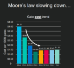
In 1963, Fairchild hired Robert (Bob) Widlar to design analog operational amplifiers using Fairchild’s digital IC process. Despite its unsuitability, Widlar, in partnership with process engineer Dave Talbert, succeeded and went on to adapt the process to produce two revolutionary parts, the world’s first operational amplifiers, the µA702 in 1964 and µA709 in 1965. With these two parts, Fairchild now dominated both the analog and digital integrated circuit markets, first with its µLogic RTL family and then with its 930 series DTL, and in April 1965 Gordon Moore famously publishing his article ‘Cramming More Components onto Integrated Circuits’ in Electronics Magazine. Later to be known as Moore’s Law, this was basically an extrapolation of four plots on a graph of IC transistor density over time.
Fairchild’s digital technology lead was, however, being overtaken by Texas Instruments who, having fallen behind in RTL and DTL, had decided to copy Sylvania’s Ultra High Performance (SUHL) transistor–transistor logic (TTL) circuit design and adapted it to its own process to counter the announcement of Fairchild’s third generation 9000 series TTL logic.
Headed up by Stewart Carrell, Texas Instruments set up a ‘design factory’ that could churn out several new designs a week, mostly by guessing the W/L ratios, laying out the circuits, correcting them if the prototypes did not work, and zeroing in on a specification that manufacturing could support. The design factory was supported by an optical photomask generator, as opposed to manual rubylith layout, that could create a photographic chip layout very quickly, and a ‘quick-turn’ fab line to rapidly turn out parts.
To strengthen their attack, Texas Instruments masterminded a marketing coup over Fairchild by persuading other semiconductor firms to second source its TTL rather than Fairchild’s competing product. In this one masterly move, Texas Instruments established its 74 Series version of TTL as the de facto third generation industry standard, leaving Sylvania’s SHUL, Fairchild’s 9000 series and other proprietary alternatives behind. It then proceeded to masterfully neutralise the entire second-source movement by providing every engineer with a copy of its ubiquitous orange book (The TTL Data Book), its twice-yearly ‘must attend’ TTL seminars in all major cities, not just in the US but globally, supported by an aggressive new product introduction programme.
By always ensuring any bill of materials (BOM) included at least one TTL part that was only available from it, Texas Instruments was able to stay one step ahead of the competition and ‘own’ the TTL market for the best part of 30 years, until standard logic eventually fell victim to the 1980’s Application Specific Integrated Circuit (ASIC) revolution.
In the meanwhile, starved of CapEx, Noyce’s position on Fairchild’s executive staff was consistently being compromised by Sherman Fairchild’s corporate interference and his lack of company support. Many of the Fairchild management team were increasingly upset by Sherman’s corporate focus on unprofitable ventures at the expense of the semiconductor division. The firm then suffered its ultimate humiliation in July 1967 when the semiconductor industry fell victim to the first of its legendary recessions, during which time the company became both unprofitable and was forced to concede its technology leadership to Texas Instruments.
Charles Sporck, Noyce’s Operations Manager, and reputed to run the tightest operation in the world, together with Pierre Lamond left in early 1968 to join the already departed Widlar and Talbert at National Semiconductor, both having grown disillusioned by the way things were going. This trigger Noyce and Moore’s departure from the firm later that same year and was to prove a pivotal moment in the eventual demise of the firm. The collective exodus of Sporck, Noyce and Moore, along with so many other iconic executives, signalled the end of an era and prompted Sherman Fairchild to bring in a new management team, led by C. Lester Hogan, then vice president of Motorola Semiconductor. Of the eight original founders only Julius Blank now remained, although he too would be gone within a year.
Hogan’s arrival, and the subsequent displacement of Fairchild managers, demoralised the firm even further, prompting a further exodus of employees to start up a host of new companies. Nicknamed ‘Hogan’s Heroes’, the ultra-conservative Motorola executives immediately clashed with Jerry Sanders III who, with his boisterous flamboyant style, was responsible for Fairchild’s sales.
Whilst initially slow to respond to the changing market, under Sander’s direction Fairchild had embarked on a strategy of leapfrogging Texas Instruments by focusing on more complex large scale (LSI), 30 plus gate parts, instead of simpler small and medium scale (SSI/MSI), under 30 gate devices, a strategy that was proving popular and successful with engineers, forcing Texas Instruments to recognize the threat and copy all of Fairchild’s 9300 series parts under 74 series numbers, for example the 9300 became the 74195 and the 9341 the 74181.
Sander’s whole strategy collapsed, however, when Hogan capitulated to Ken Olsen, founder and CEO of Digital Equipment Corporation (DEC) and a key Fairchild customer. Olsen wanted Fairchild to give up on its proprietary TTL technology and second source Texas Instruments’ 74 Series TTL instead. Against Sanders’ wishes, Hogan agreed, signing the death warrant for Fairchild’s TTL strategy. Sanders was, understandably, absolutely livid with fury. “You’ve just killed the company Ken”, Sander’s fumed.
Hogan’s betrayal was the last straw for Sanders and he, together with a group of Fairchild engineers, quit to start Advanced Micro Devices (AMD). With Sanders installed as President, one of his first moves was to declare the mantra ‘people first, revenues and profits will follow’ and give every employee stock options in the new company, an innovation at the time.
In a subsequent boardroom coup, Wilf Corrigan, who had moved with Lester Hogan as director of Discrete Product Groups, succeeded Hogan as President and CEO in 1974, but Fairchild’s fate continued to decline, dropping to sixth place in the semiconductor industry by the end of the decade.
In the summer of 1979, with the semiconductor market riding high on its fourth year of successive double-digit growth, Fairchild fell victim to a hostile takeover bid from Gould, a major US producer of electrical and electronic equipment, hell-bent on a diversification strategy.
Unable to fight off the buy-out, Corrigan elected instead to seek the best price for the shareholders and the firm was eventually sold to Schlumberger, a French oil services industry company for US$350 million or US$66 per share vs. the Gould US$54 (later increased to US$57) offer.
Schlumberger, however, proved unable to inject vitality into the deteriorating company and it continued to lose money. Corrigan departed in February 1980 and, once his one-year non-compete severance obligation was over, he and Rob Walker co-founded ASIC pioneer LSI Logic Corporation in 1981.
It initially replaced Corrigan by one of its own managers, Tom Roberts, who unsuccessfully tried to run the firm like a heavy equipment company. Two years later, in 1983, the firm finally called in Donald W. Brooks, a Texas Instruments veteran, to reverse its decline but by then Fairchild semiconductor was a legend in trouble, lagging in leading-edge technologies and losing money, even as the rest of the semiconductor industry was booming.
The firm was eventually sold to National Semiconductor in 1987 for one-third of the price paid by Schlumberger eight years earlier. With the Fairchild brand now dead, Brooks left, and the company was back in the hands of former Fairchild General Manager, Charlie Sporck.
Kirk Pond became COO at National Semiconductor in 1994 where he led the successful management buyout in 1997. With the Fairchild name revived, Pond continued as President and CEO until 2005, when he became Chairman, before retiring a year later in 2006.
He was succeeded by Mark Thompson until the firm was acquired by ON Semiconductor in September 2016. ON Semiconductor was the discrete, standard analog and standard logic device division spun out from Motorola’s Semiconductor Components Group in 1999.
The Silicon Valley Legacy. The three key inventions that changed the world in the 1960s were the integrated circuit, startup fever and venture capital. No doubt these inventions would have happened somewhere else in the world, at some other time, by somebody else, but the fact they all occurred within a short space of time, in the Palo Alto region, driven by the entrepreneurial spirit of the traitorous eight and the many other key contributors, along with the Stanford University ethos, is what made Silicon Valley so special and unique.
But what if Shockley’s parents had moved to Colorado, Nevada or West Virginia to pursue their mining careers on their return to the United States from London rather than Palo Alto? Would Silicon Valley had developed there instead?
What if Shockley had chosen to set up Shockley Semiconductors on the East Coast, where there was an already well-developed infrastructure, rather than Palo Alto which had none? From an infrastructure perspective, the East Coast was far better positioned to have hosted Silicon Valley there.
What if the Russians, Europeans or Japanese had invented the integrated circuit first? These regions were known to be working on this at the time. Could Silicon Valley have sprung up in the USSR, Europe or Tokyo instead?
What if Fredrick Terman had not had the foresight to develop a community of interest between Stanford’s faculties, industry and encourage new enterprises to cluster around the university?
What would the world look like today had any of these scenarios happened?
Clearly, fate played a role in bringing Shockley and semiconductors to Palo Alto, but the West Coast proved a far more fertile environment for the risk-taking entrepreneurial spirit of the traitorous eight and their peers than the more risk-averse and mature East Coast business and financial community.
All eight of the original founders eventually left Fairchild and went on to become serial entrepreneurs, co-founding between them a wide variety of new startups, both in semiconductors and venture capital, surrounded by brilliant engineers who wanted to start new companies, prove themselves and change the world, stoking the startup fever boom driven by Shockley Semiconductor as the embryo, Fairchild Semiconductor as the incubator and the Palo Alto infrastructure as the catalyst. The rest, as they say, is history.
The Lunch That Changed The World
On February 14, 1956, Arnold O. Beckman and William B. Shockley announced to a luncheon audience of scientists, educators, and the press at San Francisco’s St. Francis Hotel that they were founding Shockley Semiconductor Laboratory in Palo Alto, California.
The entrepreneurial spirit of the Valley, and the rise and fall of Fairchild, is best summed up by the following comment from Rob Walker, co-founder of LSI Logic: “It’s amazing what a few dedicated people can accomplish when they have clear goals and a minimum of corporate bullshit.”
Malcolm Penn
22 Dec 2021
With acknowledgment and gratitude to my many industry colleagues, old and new, who proofed early drafts and offered much-appreciated additional insights, fact checks and clarifications. Happy 74th birthday!
Also read:
Future of Semiconductor Design: 2022 Predictions and Trends
The Semiconductor Ecosystem Explained
Are We Headed for a Semiconductor Crash?