On Monday, February 7, 2022, Intel Foundry Services (IFS), made a series of major announcements regarding the RISC-V architecture and ecosystem:
- Intel will be joining the RISC-V International association with a Premier Membership, and Bob Brennan, Vice President of Customer Solutions Engineering for Intel Foundry Services, will be joining both the RISC-V Board of Directors and Technical Steering Committee.
- Intel has created a $1B strategic innovation investment fund as a collaboration between Intel’s venture capital group and IFS to support established companies and the slew of early-stage start-ups that are looking to create disruptive technologies and to foster further build-out of the RISC-V architecture and ecosystem.
- IFS launched Accelerator, a foundry ecosystem alliance with three specific areas of focus:
- The IFS Accelerator – EDA Alliance includes: Ansys, Cadence, Siemens EDA and Synopsys.
- The Accelerator – IP Alliance includes IP vendors as well as SoC silicon vendors, chiplet vendors, board vendors and accelerator manufacturers. RISC-V vendor members include Andes Technology and SiFive. Other partners in the IP Alliance: include AwaveIP, Analog Bits, Arm, Cadence, eMemory, M31, Silicon Creations, Synopsys and Vidatronic.
- The Accelerator – Design Services Alliance includes design service providers as well as cloud service providers, and the three partners are Capgemini, Tech Mahindra and Wipro.
- Finally, Intel announced that IFS is working with several cloud providers to develop an open chiplet platform for creating products with multiple types of computing processor modules aboard.
All these announcements taken together indicate just how serious Intel is in restarting their silicon foundry business and their intent to become a major player. Intel was already supporting the x86 and Arm architectures, but the addition of RISC-V indicates a serious commitment to the silicon foundry customer base and a desire to be open to new innovations going forward. In fact, Intel has already developed a RISC-V CPU as a soft processor for use in its FPGA product lines. The Nios V is based on RISC-V; the RV32IA architecture is designed for performance, with atomic extensions, 5-stage pipeline, and AXI4 interfaces. However, the current set of announcements go far beyond this soft CPU offering.
Intel’s support in these announcements of the RISC-V architecture and its evolving ecosystem further validates RISC-V as a viable counter to Arm CPUs in the marketplace and adds even more credibility to the growing momentum behind RISC-V.
The creation of an open chiplet platform is especially notable since it could mean platforms using x86, Arm and RISC-V processors all in the same product. This would be very interesting to many companies looking to accelerate their product introductions and also reduce development costs. A standard created around this concept would go far in influencing future production commitments from prospective customers looking for foundry capacity and wafer starts. Since Intel would be responsible for developing such a standard, they would likely figure prominently in the decisions reached on where to engage such technologies.
The four RISC-V IP vendors partnering with IFS – Andes Technology, Esperanto Technology, SiFive and Ventana Micro Systems – are all poised to benefit from this announcement. Their IP will be used by future IFS customers to optimize RISC-V CPU cores, chiplets and packaged products. In addition, they would likely gain access to Intel foundry capacity for their own silicon products at advanced nodes at some future point, although the current announcement does not discuss this.
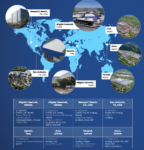
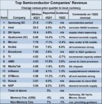
All in all, this series of announcements, adding 16 founding companies to the IFS Alliance, paint a picture of a company – Intel – that is looking to establish a serious presence in the silicon foundry business, to once again be not only a market leader (they are currently #2 behind Samsung in the 2021 revenue rankings), but to also resume their position as a thought leader in our industry. This is reminiscent of the Intel from the 1980s and 90s when Intel was driving the industry with new products and concepts. Truthfully, much of this was initially driven by the rise of the PC market and then later the rise of the internet, but there was no shortage of innovative ideas and concepts.
Today, the semiconductor market is long past being solely driven by the PC market and the internet, but new horizons beckon with AI, 5G, IoT, IIoT and automotive all poised to become the new drivers of our industry. Intel seems poised to assume a leadership position once again, and their recent commitments in terms of new fabs and capital expenditures underline these commitments. Adding support for the emerging RISC-V architecture and ecosystem back up these commitments in a very meaningful way!
However, there are other areas of the semiconductor market that are impacted by these announcements beyond the silicon foundry market.
Implications and Possibilities
The EDA Market
IFS named several EDA vendors to their Accelerator EDA Alliance – Ansys, Cadence, Siemens EDA and Synopsys. Each of these companies has a range of design tools that can be applied to silicon designs using the RISC-V architecture. Semico expects these companies will see an increased usage for their tools now that Intel is seeking new customers for its foundry services.
An added benefit to these companies is having early access to process and advanced IC packaging roadmaps, process design kits (PDKs) and technical training. This allows the EDA vendors’ R&D teams to fine-tune EDA tools and IP for the Intel portfolio of process and packaging technologies so customers can meet power, performance and area requirements.
SoC Design
SoC designs are growing around 5% – 6% per year – and this in an environment where wafer starts are constrained due to high demand. With Intel’s signal of investing in several new fabs over the next few years, and with TSMC and Samsung also committing to higher capex expenditures over the short term, Semico believes the industry can expect to see more companies undertake new design activity. Although design starts are not tied directly to wafer capacity, it does help to have a reasonable expectation that your just-completed design will find a home at one of the leading silicon foundries and have a hope of being produced in a reasonable timeframe!
The SoC Market
Creation of an open standard around a chiplet platform that embodies heterogenous CPU architectures offers the possibility of establishing new criteria for performance and flexibility in SoC silicon solutions. The emerging chiplet market already has a great deal of interest in it and momentum behind it, and the commitment to drive its evolution further will create even more support for it.
The SIP Market
More designs and more SoC silicon mean more IP being created and licensed. The chiplet phenomena is going to be one of the main drivers of the growth in this market in the coming years. With any SoC solution, IP is used in its creation, and chiplets will be no exception. As we have seen previously, designs that start out small will grow in performance and complexity over time due to evolving market requirements, requiring even more IP to accomplish. The prospect of heterogenous CPU designs based on the chiplet standard and platform Intel is looking to create could enable another uptick in IP market growth and revenue generation. Increasing complexity and performance levels usually mean more IP usage and the IP market is well-positioned to deliver on those requirements.
RISC-V International
We would be remiss if we didn’t also mention the great job the RISC-V International association has done in shepherding and guiding the organization to this point. By their steady guidance, they have enabled a new CPU architecture to take center stage in an amazingly short period of time. Their leadership should be commended for its vision and service to the semiconductor industry. Good job everyone!
The Other Shoe
“Synchronicity – describes circumstances that appear meaningfully related yet lack a causal connection.” C.G Jung. Or, nothing ever happens in a vacuum!
On Tuesday, February 8, 2022, Softbank and NVIDIA officially terminated their agreement for NVIDIA to acquire Arm. Softbank will revisit the plan to IPO Arm as a US-headquartered company set to occur sometime within their 2023 fiscal year, ending March 31, 2023.
Simon Segars has stepped down as Arm CEO and will be replaced by Rene Haas, who will oversee Arm’s IPO. Segars will “support the leadership transition in an advisory role for Arm.”
In the initial deal execution of the Purchase Agreement between SoftBank and NVIDIA, NVIDIA paid Softbank a total of $2.0B. Here is a direct quote from SoftBank’s 2021 annual report.
“Upon the execution of the Purchase Agreement on September 13, 2020, SBGC and Arm received cash totaling $2.0 billion. Of this amount, $1.25 billion was received as a deposit for part of the consideration in the Transaction (refundable to NVIDIA subject to certain conditions until the closing of the Transaction, after which such amount will become non-refundable) and $0.75 billion was received by Arm as consideration for a license agreement that Arm and NVIDIA entered into concurrently with the execution of the Purchase Agreement.”
Arm-NVIDIA acquisition, SoftBank 2021 Annual Report, page 78
The official ending of the purchase agreement is a recognition of the regulatory headwinds that were aligned against the deal and signal it is time to move to the next phase of this story – the successful IPO of Arm as an independent entity once again.
In this context, the ‘other shoe’ refers to the Intel announcements and now the Softbank-NVIDIA announcement in conjunction with each other. As far as I can see, no one has yet commented on these two events taken together. While coincidences do happen, I suspect many people will take these two events as being tied together; they very well may be, although they don’t appear to be on the surface.
Could Intel have orchestrated these announcements at this time to take advantage of the difficulties being encountered by Arm and NVIDIA? It is possible, but unlikely. The deal was either going to gain approval or not based on its own merits, and the timing of these announcements, while very interesting, is probably not connected to the approval process.
Arm–NVIDIA
Now that the acquisition is officially terminated, what is next for Arm and NVIDIA? Arm has received the $750M from NVIDIA presumably to account for licensing all of Arm’s IP in a long-term licensing arrangement and to partially offset the costs of collaboration before the two companies became one. Now that this is no longer happening, what are the likely next steps for both?
- One of the arguments Arm put forth in favor of approval was the thought that if Softbank tried to pursue an IPO for Arm, Softbank would not be able to attain the desired revenue from the IPO.
- Arm would not be able to attract the level of investment they feel is necessary to fund their future R&D efforts as an independent company.
While both these statements may be true to a degree, it seems highly unlikely that an IPO of Arm would not generate a reasonable amount of revenue. Would this be enough to satisfy Softbank? They did originally acquire Arm for $32B and would definitely want to recoup at least that sum again. The question is: can they?
Arm is the largest IP vendor today by far, and one could assume that any IPO would take that into account. Both the SoC market and the IP market are growing nicely, and as outlined above, the Intel chiplet initiative will likely add to that growth. It is likely that Softbank would garner a reasonable amount of cash from the IPO—although probably not the $32B+ they are looking for—and they could take the rest in stock in the new company. Over the long term, this would provide them the amount of money they think Arm is worth—it would just take longer than Softbank would want.
Is it unlikely that Arm, in its IPO, would not be able to generate adequate amounts of capital to fund their R&D efforts? This is more problematic. When Arm was a standalone company, they did have this problem to some degree. But that was several years ago, when Wall Street was not as in tune with the SoC, IP and AI markets as it is today. Things have changed with the rise of AI, which Arm is at the heart of with their Neoverse CPU architecture. They now have a competitor who is about to become more capable with new investments to its ecosystem. Arm will have its work cut out for it, but the company is still the market leader by a wide margin!
With the termination of the acquisition, NVIDIA’s efforts to commercialize their IP into licensable form using ARM’s expertise is going to be more difficult, but not impossible. Their efforts to move their GPU architecture SIP into SoC silicon and obtain access to some of the markets Arm serves needs to be intelligently orchestrated and managed.
Can NVIDIA still successfully commercialize its GPU as licensable IP? It is hard to believe they will be unable to do so. They could always commission Arm to do the commercialization and not need to pay $40B+ for the privilege. They already have a very tight partnership with Arm. Why not give them another $1B–$2B to complete the task if NVIDIA truly believes this is a must-have for their business going forward? It will be more difficult now, but still mostly doable.
This brings up an interesting point: Arm and NVIDIA have been working on this collaboration for approximately 18 months—how close were they to completed? Even if not fully finished, now that the deal is over, some of the IP being worked on must be close to completion even if it still needs some work. What happens to that IP? I’m sure they can’t simply abandon it – too much money and time invested. Once it is finally completed, we could see a cross-licensing deal between the two companies which would still get the NVIDIA IP into the market with some sort of revenue sharing arrangement. After all, one of the reasons NVIDIA wanted Arm was also to gain their marketing prowess and contacts to market the IP. That can still be done, but as a partnership, not as an acquisition.
It is likely that a larger loss to NVIDIA would be the lack of access to Arm’s markets—the ones that NVIDIA cannot access today. NVIDIA was looking for Arm’s expertise to take the NVIDIA GPU architecture and pare the power requirements down to something more palatable to use in the mobile market. This is probably still possible, but needs to be carefully done. Not every application requires hundreds of GPU cores, and a judicious scaling of the architecture will probably yield results that will fit into most applications as IP. Also, now that Arm and NVIDIA will remain separate companies, and NVIDIA does not absolutely need to exclusively use Arm, the door is partially open to them using one of the RISC-V CPU cores that are coming onto the market. At the end of the day, its all about fitting the right solution to the right application and a RISC-V CPU core might be one of those solutions in the future.
Conclusions
With these announcements, Intel has acted both strategically and tactically:
- Strategically, in aiding and empowering a competing architecture to Arm
- Tactically, in lining up 16 companies to support its foundry initiative
Intel satisfied many needs all at one time and have adroitly given themselves momentum for reentrance into the silicon foundry market. Now they need to execute on this vision. Given how they have handled the process so far, Semico thinks it likely they can do so!
Also read:
The Intel Foundry Ecosystem Explained
The Rising Tide of Semiconductor Cost
Podcast EP61: A deep dive on Intel and semiconductors with Stacy Rasgon