As I previously wrote about here, Intel is presenting their Intel 4 process at the VLSI Technology conference. Last Wednesday Bernhard Sell (Ben) from Intel gave the press a briefing on the process and provided us with early access to the paper (embargoed until Sunday 6/12).
“Intel 4 CMOS Technology Featuring Advanced FinFET Transistors optimized for High Density and High-Performance Computing,”
The first thing I want to discuss is the quality of this paper. This paper is an excellent example of a well written technical paper describing a process technology. The paper includes the critical pitches needed to judge process density, the performance data is presented on plots with real units and the discussion provides useful information on the process. I bring this up because at IEDM in 2019 TSMC published a paper on their 5nm technology that had no pitches, and all the performance plots were normalized without real units. In my view that was a marketing paper not a technical paper. At the conference press luncheon, I asked the organizing committee if they considered rejecting the paper due to the lack of content and they said they had but ultimately decided 5nm was too important.
Intel has disclosed a roadmap for the next four nodes (Intel 4, 3, 20A, and 18A) with dates, device types, and performance improvement targets. They are now filling in more detail on Intel 4. In contrast, Samsung is in risk starts on their 3nm and have disclosed PPA (Power, Performance and Area) targets but no other details, for 2nm they have disclosed that it will be their third generation Gate All Around (GAA) technology due in 2025 but no performance targets. TSMC has disclosed PPA for 3nm that is currently in risk starts and for 2nm a risk-start date has been disclosed but no information on performance, or device type.
Intel 4 Use Target
Before getting into the details on Intel 4, I want to comment on the target for this process. As we went through the details it became clear this process is targeted at Intel internal use to manufacture compute tiles, it is not a general use foundry process. Intel 4 is due late this year and Intel 3 is due next year; Intel 3 is the focus for Intel Foundry Services. Specifically, Intel 4 does not have I/O fins because they are not needed on a compute tile that is going to communicate solely with other chips on a substrate and Intel 4 only offers high performance cells and does not have high density cells. Intel 3 will offer both I/O fins and high-density cells as well as more EUV use and better transistors and interconnect. Intel 3 is designed to be an easy port from Intel 4.
Density
Anyone who has read my previous articles and comparisons knows I put a lot of emphasis on density. In figure 1 of the Intel 4 article, they disclose critical pitches for Intel 4 and compare it to Intel 7, see figure 1.
Figure 1. Intel 4 Versus 7 Pitches.
The high-performance cell height (CH) for Intel 7 is 408nm and for Intel 4 is 240nm. The Contacted Poly Pitch (CPP) for Intel 7 is 60 and for Intel 4 is 50, the product of CH and CPP for Intel 7 is 24,480nm2 and for Intel 4 is 12,000nm2, providing an ~2x density improvement for high performance cells. Intel 4 also provides a 20% performance per wall improvement versus Intel 7 and high density SRAMs are scaled by 0.77x.
To put this density improvement in context it is useful to better understand Intel’s recent process progression. Figure 2 summarizes four generations of Intel’s 10nm process.
Figure 2. Intel 10nm Generations.
IC Knowledge has a strategic partnership with TechInsights, we believe them to be the best in the world at construction analysis of leading-edge semiconductors. TechInsights first analyzed Intel 10nm in July 2018 and refers to this as generation 1, TechInsights completed another 10nm analysis in December 2019 finding the same density but a different fin structure leading them to refer to this as generation 2. In January 2021 TechInsights analyzed the 10nm Super Fin parts that offers a 60nm CPP option for performance along with the original 54nm CPP (generation 3). Finally in January 2022 TechInsights analyzed a 10nm enhanced Super Fin part, what Intel now calls Intel 7 (10nm generation 4). One interesting thing to me about the result of the Intel 7 analysis is TechInsights only found 60nm CPP in the logic area, no 54nm CPP and taller cells.
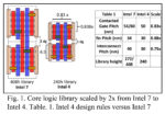
My policy for characterizing process density is to base it on the densest cell available on the process. For Intel 7 a 54nm CPP cell 272nm high is “available” but not used and the 408nm high cell with a 60nm CPP yields a transistor density of ~65 million transistor per millimeter squared (Mtx/mm2) versus ~100 MTx/mm2 for earlier generations. So how do we place Intel 4 versus prior generation processes and the forthcoming Intel 3 process, see figure 3.
Figure 3. Intel Density Comparison.
In figure 3 I have presented high-density and high-performance cell density separately. Intel 4 is ~2x the high-performance cell density of intel 7 as Intel has disclosed. Intel 3 is supposed to have “denser” libraries versus Intel 4. If I assume the same pitches but a smaller track height for Intel 3, I get ~1.07x denser high-performance cells and ~1.4x denser high-density cells versus Intel 10/7.
Another interesting comparison is Intel 4 high-performance cell size versus TSMC high performance cell sizes for 5nm and 3nm, see figure 4.
Figure 4. Intel 4 versus TSMC N3 and N5 High-Performance Cells.
TSMC N5 has a 51nm CPP and 34nm M2P with a 9.00 track high-performance cell that yields a 306nm CH and a 15,606nm2 CPP x CH. We believe TSMC N3 has a 45nm CPP and 28nm M2P, and for a 9.00 track high-performance cell that yields a CH of 252nm and a CPP x CH of 11,340nm2. For Intel 4 the CPP is 50nm and M2P is 45nm (disclosed in the briefing although not in the paper), this yields a tracks height of only 5.33 for the quoted 240nm CH and a CPP x CH of 12,000nm2. These values are consistent with a 4 designation since it slots between N5 and N3 for the leading foundry company TSMC, although it is closer to TSMC N3 than TSMC N5. We also believe Intel 4 will have performance slightly better than TSMC N3. I didn’t include Samsung in Figure 4 but based on my current estimates Intel 4 is denser than Samsung GAE3. Samsung may have a small performance advantage over Intel 4 and TSMC N3, but Intel 3 should surpass both Samsung GAE3 and TSMC N3 for performance next year.
I am surprised that Intel’s high-performance cell works out to just over 5-tracks in height but that is the math for the disclosed cell height and M2P.
DTCO
From a Design-Technology-Co-Optimization (DTCO) perspective Intel 4 has 3 improvements over Intel 7:
- Contact Over Active Gate is optimized for Intel 4.
- Diffusion break by dummy gate removal used to need two dummy gates (double diffusion break), Intel 7 went to 1 (single diffusion break).
- The n to p spacing used to be two fin pitches and is now 1 fin pitch. When we talk about CH in terms of M2P and tracks it is easy to forget that the devices have to fit into that same height and figure 5 illustrates how n to p spacing contributes to cell height.
Figure 5. Cell Height (CH) Scaling.
During the briefing Q&A there was a question about cost per transistor and Ben said that cost per transistor went down for Intel 4 versus Intel 7.
Performance
Intel 10/7 offered 2 threshold voltage (2 PMOS and 2 NMOS = 4 total) and 3 threshold voltage (3 PMOS and 3 NMOS = 6 total) versions. Intel 4 provides 4 threshold voltages (4 PMOS and 3 NMOS = 8 total). This results in ~40% lower power and ~20% higher performance.
I believe the drive current values mentioned during the briefing are 2mA/μm for PMOS and 2.5mA/μm for NMOS.
EUV usage
EUV is used in both the backend and front end of the process. Intel has focused EUV use on where a single EUV exposure can replace multiple immersion exposures. Even though an EUV exposure is more expensive than an immersion exposure, replacing multiple immersion exposures with associated deposition and etch steps can save cost, improves cycle time and yield. In fact Ben mentioned single EUV exposures resulted in 3-5x fewer steps in the sections that EUV replaced. Intel 7 to Intel 4 see a reduction in masks and step count. In the front end of line EUV is focused on replacing complicated cuts, gate or contact. Intel didn’t explicitly disclose that EUV is used in fin patterning but we believe for Intel 7 fin patterning involved a mandrel mask (Intel calls this a grating mask) and 3 cut masks (Intel calls these collection masks). For Intel 4 this could easily have transitioned to 4 cut masks. Without naming the layer replacing 4 cut masks with a single EUV mask was mentioned and we believe this could be where that happens.
In the paper Intel mentions that M0 is quadruple patterned. For Intel 10/7 Intel also disclosed quadruple patterning and TechInsights analysis showed that 3 block masks were needed. It is possible that Intel 4 would need 4 block masks for M0 and this may be another place where EUV eliminate 4 cut/block masks.
A gridded layout was used for interconnect to improve yield and performance.
We believe there are ~12 EUV exposures used in this process, but this was not disclosed by Intel.
Interconnect
It is well known that Intel went to cobalt (Co) for M0 and M1 at 10nm. Co offers better electromigration resistance than copper (Cu) but higher resistance (Authors note, electromigration resistance of a metal is proportional to melting point). For Intel 4, Intel has gone to an “enhanced” Cu scheme where pure Cu is encased in Co (in the past Intel doped the Cu). A typical flow to encapsulate Cu in Co is to put down a barrier layer with a Co layer to serve as the seed for plating. Once plating is complete and planarized to form an interconnect the Cu is capped with Co. This process results in slightly degraded electromigration resistance versus Co but still above the 10-year lifetime goal and the resistance of the line is reduced. In fact, even though the interconnect lines are narrower for Intel 4 versus Intel 7, the RC value are maintained.
The process has 5 enhanced copper layers, 2 giant metal layers and 11 “standard” metal layers for a total of 18 layers.
MIM caps
With the increasing importance of power delivery Metal-Insulator-Metal (MIM) capacitors are used to reduce power swings and have undergone continuous improvement. For Intel’s 14nm process 37 fF/μm2 was achieved, this improved to 141 fF/μm2 for 10nm, 193 fF/μm2 for intel 7 and has now been increased ~2x to 376 fF/μm2 for Intel 4. Higher values enable MIM capacitors with more capacitance improving power stability without taking up excess space.
Where they went wrong
During the Q&A Ben was asked where Intel went wrong in the past, he said that in the past Intel tried to do too much at once (authors note, for example Intel 22nm to 14nm was a 2.4x density increase and then 14nm to 10nm was a 2.7x density increase, see figure 3. Intel has now adopted a modular approach where you can separately develop modules and deliver more performance, more quickly.
When asked what he was most proud of, he said achieving yield and performance with library scaling and the process looks good in factories. The process is simpler with EUV improving yield and reducing registration issues.
Production sites
Also during the Q&A Ben was asked about production sites. He said initial production will be in Hillsboro followed by Ireland. He said they haven’t disclosed additional production plans beyond that.
In our own analysis of EUV availability we have published here that EUV exposure tools will be in short supply for the next few years. This is also consistent with Pat Gelsinger discussing tool shortages for Intel’s new fabs. We believe EUV tool availability will gate Intel’s fab ramp. Furthermore we believe Intel has ~10 to 12 EUV tools presently and until recently they were all in Hillsboro. One of those tools has now been moved to Fab 34 in Ireland and we believe that as intel receives further EUV tools this year they will be able to ramp Fab 34 up. Late this year we expect Fab 38 in Israel to begin ramping and our belief is that will be the next Intel 4/3 production site. Following that in the later part of 2023, Fabs 52 and 62 in Arizona should start receiving EUV tools. We also believe most of this capacity will be needed for Intel’s own internal use and they will have limited EUV based foundry capacity until the 2024/2025 timeframe.
Yield and Readiness
Throughout the briefing everything we heard about yield is that it is “healthy” and “on schedule”. Meteor Lake compute tiles are up and running on the process. The process is ready for product in the second half of next year.
Conclusion
I am very impressed with this process. The more I compare it to offerings from TSMC and Samsung the more impressed I am. Intel was the leader in logic process technology during the 2000s and early 2010s before Samsung and TSMC pulled ahead with superior execution. If Intel continues on-track and releases Intel 3 next year they will have a foundry process that is competitive on density and possibly the leader on performance. Intel has also laid out a roadmap for Intel 20A and 18A in 2024. Samsung and TSMC are both due to introduce 2nm processes in the 2024/2025 time frame and they will need to provide significant improvement over their 3nm processes to keep pace with Intel.
Also Read:
An Update on In-Line Wafer Inspection Technology
0.55 High-NA Lithography Update
Intel and the EUV Shortage