TSMC presented two papers on 3nm at the 2022 IEDM; “Critical Process features Enabling Aggressive Contacted Gate Pitch Scaling for 3nm CMOS Technology and Beyond” and “A 3nm CMOS FinFlexTM Platform Technology with Enhanced Power Efficiency and Performance for Mobile SOC and High Performance Computing Applications”.
When I read these two papers prior to the presentations, my initial reaction was the first paper was describing TSMC’s N3 process and the second paper is describing the N3E process, this was confirmed by the presenter during the second presentation.
My second reaction was these papers continue TSMC’s habit of minimizing the amount of technical detail they present. As I discussed about TSMC’s 5nm paper in 2019 here there is minimal critical pitch information and in 2019 all the electrical results were normalized. In these two papers the electrical results are at least in real units, but the first paper only has Contacted Gate Pitch and the second paper only has a minimum metal pitch. I find this very frustrating, the critical pitches will be measured and disclosed as soon as parts hit the open market and insiders and TSMC’s competitors likely already know what they are, I don’t see how presenting a quality technical paper would be a problem. When Intel presented Intel 4 at the VLSI Technology Symposium last year they presented an excellent paper with all of the key data (I wrote about that paper).
N3 Paper
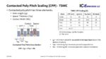
In the first paper, a Contacted Gate Pitch (Contacted Poly Pitch, CPP as I describe it) of 45nm is disclosed. CPP is made up of Gate Length (Lg), Contact to Spacer Thickness (Tsp), and Contact Width (Wc), as illustrated in figure 1.
Figure 1. CPP.
From figure 1. We can see TSMC has been reducing CPP for each new node by reducing all three elements that make up CPP. Logic designs are done by using standard cells and CPP is a major driver of standard cell width, therefore shrinking CPP is a key part of improving density for a new node.
Minimum Lg is a function of gate control of the channel, for example moving from single gate planar devices with unconstrained channel thickness to FinFETs with 3 gates surrounding a thin channel enabled shorter Lg. Gate control of a FinFET is weakest at the base of the fin and optimization is critical. Figure 2 illustrates DIBL versus Lg for multiple TSMC nodes and also how optimizing the fin reduced DIBL for the current work.
Figure 2. DIBL versus Lg.
The second element in shrinking CPP is the Tsp thickness. Reducing Tsp drive up parasitic capacitance unless the spacer is optimized to lower the k value. Figure 3 illustrates TSMC’s investigation of low-k spacers versus an air gap spacer. TSMC found that a low-k spacer was the best solution for scaled CPP.
Figure 3. Contact to Gate Spacer.
The final element of CPP is contact width. In this work an optimized self-aligned contact (SAC) scheme was developed that provided lower contact resistance. The left side of figure 4 illustrates the SAC and the right side illustrates the resistance improvement.
Figure 4. Self-Aligned Contact.
This work enabled the N3 process with a high-density SRAM size of 0.0199μm2. This work will also be important as TSMC moves forward to their 2nm process. At 2nm TSMC is going to move to a type of gate-all-around (GAA) architecture known as a horizontal nanosheet (HNS) and HNS enables shorter Lg (4 gates instead of three surrounding a thin gate), but Wc and Tsp will still have to be optimized.
N3E
The N3E process is described by TSMC as an enhanced version of N3, interestingly N3E is believed to implement relaxed pitches versus N3, for example CPP, M0 and M1 are all believed to be relaxed for performance and yield reasons. There are varying stories about TSMC N3 and whether it is on time or not. The way I look at it is N5 entered risk starts in 2019 and by Christmas 2020 there were Apple iPhones in store with N5 chip. N3 entered risk starts in 2021 and iPhones won’t hit the market with N3 chips until next year. In my view the process is at least 6 months late. In this paper a high-density SRAM cell size of 0.021 μm2 is disclosed. Larger than the N3 SRAM cell of 0.0199 μm2. The yields for N3 are generally described as being good with 60% to 80% mentioned.
There are two major features of this process discussed in this paper:
- FinFlexTM
- Minimum metal pitch of 23nm with copper interconnect with an “innovative” liner for low resistance.
FinFlexTM is a kind of mix and match strategy with double height cells that can be 2 fins cells on top with 1 fin cells on the bottom for maximum density, 2 fin cells over 2 fin cells as kind of mid performance and density and 3 fin cells over 2 fin cells for maximum performance. This give designers a lot of flexibility to optimize their circuits.
Figure 5 illustrates the various FinFlexTM configurations and figure 6 compares the specifications for each configuration to a standard 2 over 2 fin cell at 5nm.
Figure 5. FinFlexTM cells.
Figure 6. 3nm FinFlexTM cell performance versus 5nm cells.
A plot in this paper is the via resistance distribution for the 15 level metal stack at approximately 550 ohms. In current processes power comes in through the top of the metal stack and has to travel through the via chain down to the devices, 550 ohms in a lot of resistance in a power line. This is why Intel, Samsung and TSMC have all announced backside power delivery for their 2nm class processes. With extreme wafer thinning the vias bringing power in from the backside should offer a >10x improvement in via resistance.
Comparisons
One question you may have as a reader is how this process compares to Samsung’s 3nm process. TSMC is still using FinFETs while Samsung has transitioned to GAA – HNS they call multibridge.
At 5nm by our calculations TSMC’s densest logic cells are 1.30x the density of Samsung’s densest logic cells. If you look at TSMC density values in figure 6., the 2-2 fin cells are 1.39x denser than 2-2 cells in 5nm, and the 2-1 cells offer a 1.56x density improvement. Samsung has two versions of 3nm with the SF3E (3GAE) version 1.19x denser than 5nm and the SF3 (3GAP) version 1.35x denser than 5nm, falling further behind TSMC’s industry leading density. I also believe TSMC has better performance at 3nm and slightly better power although Samsung has closed the power gap likely due to the HNS process.
Also Read:
IEDM 2022 – Ann Kelleher of Intel – Plenary Talk