Bronco Webinar 800x100 1

Not me. Who owns IP quality?

Not me. Who owns IP quality?
by Paul McLellan on 03-05-2012 at 4:32 pm

Now that the dominant approach to building an SoC is to get IP from a number of sources and assemble it into a chip, the issue of IP quality is more and more critical. A chip won’t work if the IP doesn’t work, but it is quite difficult to verify this because the SoC design team is not intimately familiar with the IP blocks since nobody on the team designed them.

At DATE next week in Dresden there is a panel session on just this topic, moderated by Gary Smith. It takes place from 13:15 to 14:15 (or 1.15pm to 2.15pm for Americans) in the Exhibition Theater.

Participating on the panel are:

  • Fahim Rahim, director of engineering at Atrenta in Grenoble
  • Simon Butler, CEO of Methodics in San Francisco
  • Gabriele Saucier, president of D&R in Grenoble
  • Andreas Bruning, director of the technology office of ZDMI in Dresden
  • Gerd Teepe, director of design enablement for GlobalFoundries in Dresden

While there are many tools available to help verify, debug, assemble and otherwise manipulate IP, there’s a distinct lack of a solid design data management system to address the specific needs of SoC designers. As a result, IP often suffers from a bad rap regarding quality. Users blame providers, and tool vendors and CAD managers are often caught in the middle, trying to put together solutions that track changes, use models and offer some degree of version control. Complicating matters is that the term “IP quality” has different meanings to different people – is it 1) the functional correctness of the IP – does it work they way it is supposed to (i.e. bug free); 2) or defined by its ability to do what is expected with respect to design parameters – power, timing, area, etc?

The panel will discuss what needs to be done to improve the design environment from the perspective of all the players

And if you are at DATE in Dresden, there is an interesting piece of “design re-use” that is worth a visit, the Frauenkirche, destroyed by bombing in 1945. The first time I went to Dresden was still a ruin, but it has been completely rebuilt. The original was built in 1726-43 and has been rebuilt using the original plans, many of the original stones (you can tell the old from the new because they are charred). In 2003 it was half built when I took the second photo. It reopened in 2005, 60 years after it collapsed. Wikipedia page here.


Atrenta/TSMC Soft-IP Alliance: 10 companies make the grade

Atrenta/TSMC Soft-IP Alliance: 10 companies make the grade
by Paul McLellan on 03-05-2012 at 7:30 am

Last May, Atrenta and TSMC announced the Soft-IP Alliance Program which uses SpyGlass and a subset of its GuideWare reference methodology to implement TSMC’s IP quality assessment program. TSMC requires all soft-IP providers to reach a minimum level of completeness before their IP is listed on TSMC online. Since TSMC is so dominant in the foundry business right now (Global struggling with process, Intel talking the talk but not yet really walking the walk, UMC…whatever happened to them anyway?) getting approved and listed with TSMC is extremely important.

Atrenta put everything needed to meet TSMC’s requirements in an IP Handoff Kit. Under the hood this uses SpyGlass’s RTL analysis suite to check for syntax and semantic correctness, simulation-synthesis mismatches, connectivity rules, clock domain crossings, test coverage, timing constraints and…lots more.

Suk Lee of TSMC (my successor at running IC marketing when we were both at Cadence) sees this as measurably improving IP quality. Of course TSMC isn’t directly responsible for IP quality but if IP fails and chips don’t go into production TSMC don’t make any money. Anyway, ten companies have now jumped through all the hoops and qualified their IP for inclusion in the TSMC 9000 IP library.

The companies in this initial program are a veritable who’s who of the IP world (with the notable exceptions of ARM and Synopsys). In alphabetical order so as not to offend anyone:

  • Arteris (NoC)
  • CEVA (DSP cores)
  • Chips&Media (video IP)
  • Digital Media Professionals (graphics IP)
  • Imagination Technologies (GPU cores)
  • Intrinsic-ID (security IP)
  • MIPS Technologies (CPU cores)
  • Sonics (NoC)
  • Tensilica (reconfigurable processors and cores)
  • Vivante (GPU cores)

Now that the dominant way to build an SoC is through assembling IP, the issue of IP quality is is a huge problem and a mixture of tools, methodologies, standards and certification is for sure the way to address it.


Verdi’s 3rd Symphony

Verdi’s 3rd Symphony
by Paul McLellan on 03-05-2012 at 7:00 am

The first version of the debug platform Verdi (then called Debussy) dates back to 1996 over 15 years ago. The second version was released in 2002. And now SpringSoft is releasing the 3rd version Verdi[SUP]3[/SUP]which is a completely new generation. A tool environment like Verdi seems to need to be completely refreshed about every 5 or 6 years to take account of the changes in the scale of design and the issues which have become important.

The motivation for creating Verdi[SUP]3[/SUP] is to fit in with how engineers on today’s design teams work. The debug tasks vary widely depending on the company’s methodology and flow, the attributes of the design, what needs to be done, and the engineer’s job-function, experience and style. There are three themes in the changes to the platform:

  • new user-interface and personalization capabilities
  • open platform for interoperability and customization
  • new infrastructure for performance and capacity improvements

Personalization means tailoring the appearance and layout of the tool to the way that you want to work to accomplish the task at hand.


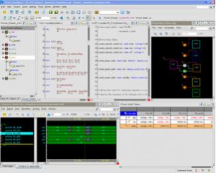
Customization is the capability to change or add to the functions available such as adding automation to perform a repetitive task, or integrating proprietary tools into the environment. Of course there is also functionality available from 3rd parties too, not to mention the VIA website announced last year. The extensibility is built on top of VIA (Verdi Interoperability Apps) making it easy to plug-in in-house tools, add items to menus, create hot-keys and so forth. For example, above the environment has been configured for power analysis.

The new user-interface is more modern and cleaner. Gone are the overlapping windows with information regularly buried out of sight. Instead the interface is now tiled so everything is within sight. Plus there are some big incremental capabilities such as being able to have multiple source-code windows open at the same time (the older version of Verdi only allowed one). A powerful search capability makes finding anything easy. Above is a comparison of the old user interface (on the left) and the new (on the right).

The basic infrastructure has been refreshed. A new parser lifts restrictions from the old one, is multi-threaded and generally faster. The FSDB (simulation data) has been compressed by 30% compared to the previous version, and also reads twice as fast on a typical 4-core configuration.

So, Verdi[SUP]3[/SUP] is a rebuild of Verdi from the ground up, with major developments in productivity, a much richer capability for customization and higher performance and capacity.

Verdi[SUP]3[/SUP] is in general beta which means all existing customers have access today and can go and download the beta release. Official first customer ship is in April.

If you are just interested in finding out more, the Verdi[SUP]3[/SUP] product page is here.


TSMC 28nm Yield Explained!

TSMC 28nm Yield Explained!
by Daniel Nenni on 03-04-2012 at 4:00 pm


Yield, no topic is more important to the semiconductor ecosystem. After spending a significant part of my career on Design for Manufacturability (DFM) and Design for Yield (DFY), I’m seriously offended when semiconductor professionals make false and misleading statements that negatively affects the industry that supports us.
Continue reading “TSMC 28nm Yield Explained!”


The 2012 International Conference on ENGINEERING OF RECONFIGURABLE SYSTEMS AND ALGORITHMS – ERSA’12

The 2012 International Conference on ENGINEERING OF RECONFIGURABLE SYSTEMS AND ALGORITHMS – ERSA’12
by Daniel Nenni on 03-03-2012 at 9:55 am


July 16-19, 2012, Monte Carlo Resort, Las Vegas , Nevada , USA

ERSA-News: ERSA-NEWS ERSA’12 Website: http://ersaconf.org/ersa12

Continue reading “The 2012 International Conference on ENGINEERING OF RECONFIGURABLE SYSTEMS AND ALGORITHMS – ERSA’12”


CEO Forecast Panel

CEO Forecast Panel
by Paul McLellan on 03-02-2012 at 2:40 pm

This year’s CEO forecast panel was held at Silicon Valley Bank. Bankers live better than verification engineers, as if you didn’t know, based on the quality of the wine they were serving compared to DVCon.

This year the panelists were Ed Cheng from Gradient, Lip-Bu, Aart and Wally (and if you don’t know who they are you haven’t been paying attention) and Simon Segars of ARM (not their CEO, of course). Ed Sperling moderated. Somebody had managed to dig up the fact that at the start of his career he’d been a crime reporter, so that made sure that we only got truthful answers all evening!

The format was completely different from prior years. Instead of each CEO getting up and doing a presentation, instead various questions were discussed. The CEOs had been polled beforehand on their answers and then EDAC members (I’m not sure how many or who, it was a bit unclear) had also been polled. So one of the interesting things was to focus on areas where the CEOs differed from the man-in-the-street. And by ‘man in the street’ I mean design engineers. You’ll get some pretty odd looks even in silicon valley asking a random person in the street when stacking die will go mainstream.

Q1: when will stacking die become mainstream?CEOs were more conservative that their customers, with CEOs going for 2015-2016 and customers with 2013. Although as Ed Cheng pointed out, what does mainstream mean? There are stacked die in most cameras, in most DRAM assemblies and so on already. Everyone agreed that memory on processor, and 2.5D interposer would arrive long before true 3D (meaning punching TSVs through active area all over the die).


Q2: what is the most difficult challenge?
CEOs went with integration, but their customers picked software, time-to-market, power and cost. Typing this now I’m not sure if the CEOs meant integration of their tools or integration of IP etc on chips. Certainly in the big EDA companies, integrating tools to work smoothly together now that they have to look forward and back up and down the tool chain is a major challenge.

Q3: what is the most prevalent concern for EDA customers?Everyone picked power, so at least the CEOs understand something about their customers. The CEOs also picked performance but their customers were more concerned with area/cost. Power is an issue right from the architectural level where people are looking for 5-10X reduction (hmm, that’s going to be tough) all the way down to the process where FinFETs are coming, soon if you are Intel, and in a couple of years if you are not.

Q4: what technology challenge will spur the next growth in EDA?Survey says…IP reuse and integration for the CEOs, and hardware/software co-design for the customers. Wally pointed out, as he has several times before, the suprising fact that all the growth in EDA, all of it, comes from new technologies. Something new comes along like place and route, grows fast and then plateaus for a decade while something new builds growth on that base.

Q5: what will EDA look like in 5 years?CEOs picked the same number of major companies but defined differently. Customers predict more startups and more consolidation. Wally noted that the top 3 EDA companies have made up 75% of EDA revenue for 40 years and that will continue although which 3 companies may change (I guess Wally can take pride in being the only member of the DMV, Daisy, Mentor, Valid that survived). Lip-Bu said that some VCs are starting to come back to EDA. I have to say that any companies I’ve been involved with have not seen any signs of this (my feeling is that EDA compaies don’t need enough money to be interesting to most funds, and the exits are too low).

Q6: where will the majority of leading edge designs be done in 5 years?EDA CEOs all picked North America, but about 30% customers picked China. Everyone agreed that on a 10 year timescale, things are a lot less certain. Aart said that a country (think China) goes through 3 stages: competing on cost, competing on competence and finally competing on creativity. China is moving from the cost to the competence era at the moment, I guess.


Q7: who will drive the industry in 5 years?
Everyone said system/software companies, but the CEOs also had some love for fabless companies and the customers for foundries and IDMs. To some extent the answer is ‘all of the above’ of course but you can’t ignore system companies, Apple in particular, due to scale. Apple increased its revenue last year by roughly Intel’s revenue. It is an unequal battle.

Q8: will SoCs rely on more cores in a single processor or more processors in 5 years?Pretty much everyone reckoned both, more cores and more processors. The big challenge here is the dreaded dark silicon. We can put the cores on there but can we power them all up?

There were a few questions from the audience. Peggy Aycinena asked that, since this was a forecast panel, what was the forecast for 2012. All the CEOs had given guidance in recent conference calls and Synopsys and Mentor predicted 8.4% and Cadence 8.8%.



Farm Management

Farm Management
by Paul McLellan on 03-01-2012 at 5:34 pm

Every so often I come across a new company in EDA or one of its neighboring domains, new to me anyway, and new to SemiWiki. One such company is RunTime Design Automation (RTDA). They provide a suite of tools for managing server farms (or internal clouds which seems to be the trendy buzzword du jour). Running a few EDA scripts on a few servers is something that is not too hard to do, but when you are looking at running tens of thousands of jobs on thousands of servers, you have a whole new set of problems. Servers crash or hang. Tools run out of licenses. Jobs depend on each other in a complicated tree. These are the problems that RTDA addresses.

When I was at Ambit we had a Q/A farm of 40 Sun workstations and 20 HP workstations, an unusually large investment at the time. Now this is a trivially small farm in an era when data-centers may house 100,000 servers and literally millions of jobs a day need to be scheduled.

RTDA have four products:

  • LicenseMonitor
  • NetworkComputer
  • FlowTracer
  • WorkloadAnalyzer


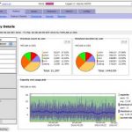
The simplest product is LicenseMonitor. It pulls license usage data from the license servers used by EDA (and other) tools, such as FLEXlm. This gives a summary of what license usage really is so that a company does not end up either having too few licenses and thus wasting time when running jobs, or having too many licenses and wasting money. It also interfaces with Network Computer to ensure jobs are not scheduled until licenses are available.


NetworkComputer is the highest performance job scheduler to spread a workload over a large server farm. It is similar to the well-known LSF but more powerful and better integrated with EDA license management. It has a GUI that allows a user to keep track of thousands of jobs, which are color coded as they become runnable, start to run, crash, complete and so forth. It can handle millions of jobs on thousands of processors. It can get license usage of, for example, simulation licenses up to very close to 100%.


FlowTracer is a much more sophisticated tool like the Unix make command that manages complex design flows, handing all the dependencies, errors and so on. It handles the entire design flow giving visibility to what is happening and automatically updating dependencies intelligently.

Finally, WorkloadAnalyzer is a server farm simulation allowing efficient compute farm planning, answering questions such as what would happen if additional servers or additional licenses were purchased. It can be used daily for planning or annually to provide data for license renegotiation. It can take information from Network Computer (or its competitors) and analyze how that workload would run under different circumstances and thus make it easier to optimize the investment.

Download the free e-book, The Art of Flows here


3D Transistor for the Common Man!

3D Transistor for the Common Man!
by Daniel Nenni on 03-01-2012 at 3:28 pm

The 1999 IDM paper Sub 50-nm FinFET: PMOSstarted the 3D transistor ball rolling, then in May of 2011 Intel announceda production version of a 3D transistor (TriGate) technology at 22nm. Intel is the leader in semiconductor process technologies so you can be sure that others will follow. Intel has a nice “History of the Transistor” backgrounder in case you are interested. Probably the most comprehensive article on the subject was just published by IEEE Spectrum “Transistor Wars: Rival architectures face off in a bid to keep Moore’s Law alive”. This is a must read for all of us semiconductor transistor laymen.

My first pick of talks at this month’s Common Platform Technology Forumwill be given by Dr. Greg Yeric, ARM Consultant Design Engineer, R&D. Greg has 20 years of semiconductor experience beginning with Motorola/Freescale, HPL, which brought him to Synopsys through acquisition, and for the last 4+ years he has been at ARM. Greg’s talk “IP Design and the FinFET Transition”will cover foundry access to finFETs. Here is a reprint of an interview with Greg from the Tech Design Forum Newsletter in case you have not seen it:

TDF: What is the big deal about finFETs and what do they mean for IP?

FinFETs hold the promise of being fundamentally better switches than bulk planar transistors. So, they’ll allow favorable power and performance scaling beyond 20nm. However, they are a new kind of transistor with new issues and limitations. They are different enough that one runs the risk of producing sub-optimum IP without good understanding and planning. But properly executed, they’ll mean that 14nm delivers better power and performance.

How big a change are finFETs?

On one hand, they have the same metal-oxide-semiconductor structure, simply folded up, accordion-style, to provide a higher current density. In that sense, designers will see them behave in familiar ways. The key change will be a sizeable bump in the roadmap for some scaling parameters. There’ll be enough notable differences that the transition should offer an opportunity to assess the scaling of our designs.

What specifically should designers be aware of?

Most everyone has heard about quantization – that the finFET drive strength is varied by the number of discrete fins in parallel. For that reason and others, low power designers will face a different granularity in choices than they’ve been used to. Another potentially more interesting side-effect of quantization is a new fin-metal gear ratio. Designers must plan for the fact that finFETs offer a change in the scaling compared to recent nodes. Delay and power can be improved in aggregate, but their components, represented by CV/I and CV^2f, will scale in different ways. I wouldn’t recommend a lazy extrapolation of past trends.

What other differences might there be?

The variability signature will probably change. finFETs improve some aspects of variability but because they have new process components, I’d expect to see other new variation issues. This shift might foretell a change in the balance between local and global variation that will affect memory and logic differently. Also, scaling to 14nm in and of itself won’t be easy, and all of the finFET issues will have to be folded – no pun intended – into this broader context. I’ll discuss a broader process scaling perspective at the forum.

My big question is parasitic extraction of 3D Transistors, how is that going to work?


2012 semiconductor market could decline by 1% or more

2012 semiconductor market could decline by 1% or more
by Bill Jewell on 02-29-2012 at 6:00 pm

The world semiconductor market grew a slight 0.4% in 2011, according to WSTS. In early 2011, expectations were for growth in the 6% to 10% range. Various natural and man-made disasters lead to weaker than expected growth. The March 2011 earthquake and tsunami in Japan disrupted semiconductor and electronics production. Floods in Thailand in 3Q and 4Q 2011 severely impacted hard disk drive manufacturing. The European financial crisis resulted in weak demand in 4Q 2011.
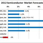
Recent forecasts for the 2012 semiconductor market are primarily in the range of 2% to 3%. Always optimistic Future Horizons predicted 8% growth. IC Insights projected 7% growth for the IC market. We at Semiconductor Intelligence believe the 2012 semiconductor market will see a slight decline of about 1%. The decline is expected due to the overall economic outlook in 2012 and the quarterly pattern of the semiconductor market. (Cick to enlarge images)

The International Monetary Fund’s (IMF) January 2012 forecast was for World GDP growth of 3.3% in 2012, half a point slower than estimated 3.8% growth in 2011. The U.S. is expected to maintain moderate 1.8% growth in 2012, the same as in 2011. The Euro Area is projected to see a 0.5% drop in GDP in 2011 due to the financial crisis. Japan’s GDP should rebound from a 0.9% decline in 2011 to 1.7% growth in 2012 as it recovers and rebuilds from the 2011 disasters. China remains a major growth driver, with expected 8.2% growth in 2012, one point lower than in 2011. Hong Kong, South Korea, Singapore and Taiwan collectively should see 3.3% growth in 2012, slowing from 4.2% in 2011.

The semiconductor market declined 7.7% in 4Q 2011 from 3Q 2011, due largely to the floods in Thailand and weakness in Europe. The largest semiconductor companies providing guidance generally expect significant revenue declines in 1Q 2012 from 4Q 2011. Intel, Texas Instruments, ST Microelectronics and AMD all gave similar revenue guidance: worst case declines of 10% to 12%, best case declines of 4% to 5%, and midpoint declines of 7% to 8%. Renesas and Broadcom also expect declines in 1Q 2012. Samsung did not give specific guidance, but expects a weak DRAM market in 1Q 2012. A couple of companies expect increases. Toshiba expects a recovery to 15.5% revenue growth for its semiconductor business after a 19% decline in 4Q 2011. The midpoint of Qualcomm’s guidance is for 2.5% growth.

We at Semiconductor Intelligence are forecasting a 5% decline in the semiconductor market in 1Q 2012. With a 5% 1Q 2012 decline following the 7.7% decline in 4Q 2011, it will be difficult for the industry to achieve positive growth for the year 2012. The average quarter-to-quarter growth rate in 2Q through 4Q 2012 would need to be 6.5% just to achieve 0% for the year. Our forecast of a 1% decline in 2012 is based on average growth of about 5% for the last three quarters. Further deterioration in the world economic situation from current expectations could result in a more significant decline in the semiconductor market in 2012 of 5% or more.