Bronco Webinar 800x100 1

Formale Verifikation in München

Formale Verifikation in München
by Paul McLellan on 03-08-2012 at 9:00 am

With DATE next week in Dresden, all eyes turn to Germany. Not to be left out, Jasper has a seminar on formal verification coming up on March 19th in the Kempinski Hotel at Munich airport. Unlike most “airport” hotels the Kempinski is indeed right in the heart of the airport. And for those of us who like a good German beer, the airport also contains a micro-brewery Airbräu where they brew their own beer in the airport, which I believe is unique.

Breakfast and lunch are provided, although I very much doubt that they serve the traditional Bavarian breakfast of beer and weisswurst. What they do serve, though, is lots of useful information about formal verification:

  • Formal verification of RTL blocks
  • Debug and design exploration
  • Post – silicon debug and root cause analysis
  • Verification of ARM-protocol based SoCs (AXI, AMBA, AHB, ACE)
  • Verification of SoCs with complex memory sub-systems (DDRxx)
  • SoC and IP connectivity
  • Control status registers
  • Closure and coverage
  • Clock domain crossing
  • X-propagation
  • Verification of designs including power-management structures


TSMC absolutely did NOT halt 28nm production!

TSMC absolutely did NOT halt 28nm production!
by Daniel Nenni on 03-07-2012 at 6:18 pm

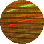
Once again industry professionals get duped! Tabloid journalism runs amok inside the semiconductor ecosystem! As if our industry does not face enough challenges, why are we wasting time on drivel like this? This is a TSMC 28nm wafer by the way and thousands of them are being shipped around the world, believe it.
Continue reading “TSMC absolutely did NOT halt 28nm production!”


CDNLive: two days of all things Cadence

CDNLive: two days of all things Cadence
by Paul McLellan on 03-07-2012 at 4:17 pm

Next Tuesday and Wednesday, March 13-14th, is CDNLive in Silicon Valley at the DoubleTree Hotel (which I see we are now meant to call DoubleTree by Hilton, although I still have to think twice not to call it the Red Lion, the group whose CFO at one point was Ray Bingham who was CFO and then CEO of Cadence. Trivia fact for the day).

CDNlive has a new format and going forward it will be much more technically focused. In the early days of CDNLive, which was the Fister era, CDNlive was modeled on the Intel developer forum. But Cadence markets to engineers who want to know about technology and practical techniques. So most of the people at CDNLive are users and relatively few Cadence people. Of the 90 sessions taking place over the two days, 76 are user-driven.

There are 3 keynotes on the first day, starting at 10.30:

  • Lip-Bu Tan, Cadence CEO Challenges, opportunities and collaboration
  • Rick Cassidy, President of TSMC North America Life in the silicon century
  • Tom Lantzsch, Exec VP of ARM Corporate Development Your world at your fingertips

Following that at noon a buffet lunch is served in the expo hall where Cadence has a booth with 14 demos and partners from ANSYS to TSMC also have booths and demos. Lunch during the second day offers a chance to meet R&D engineers from Cadence.

Before the keynotes, and after lunch, and through all of the second day, there are 8 tracks of detailed technical presentations running in parallel. The tracks are:
[LIST=1]

  • Digital Design
  • Mixed-signal/Low Power
  • Custom
  • Verification
  • SoC/DIP
  • System/Software
  • System Verifcation
  • High Performance

    Companies presenting include Cadence (of course), TSMC, Qualcomm, Broadcom, IBM, Cisco, AMD, Xilinx, ARM, Rambus and many others. A lot of customers designing chips on the leading edge with stories from the trenches.

    At the end of the day, back to the expo for a reception from 5.45 to 7.30. Demos and drinks.

    More information about the conference is here.
    Registration is here, or if you really procrastinate you can register on the day.


  • Kathryn Kranen Interview in San Jose Mercury News

    Kathryn Kranen Interview in San Jose Mercury News
    by Paul McLellan on 03-07-2012 at 1:22 pm

    There is an interview in the San Jose Mercury News with Kathryn Kranen, Jasper’s CEO. Of course the Mercury is a general newspaper and can’t expect most of its readership to have a clue what EDA is, never mind formal verification. It’s a similar problem to the one we all have when we try and explain to our families just what we do. Steve Johnson does his best to understand.

    Q: Say a company designs a new chip for an automobile. How would your formal-verification software prevent the design from having a glitch that blows a car fuse, for example?
    A: What we do is all mathematical. We can just say there is a rule, or it’s called a property, that this fuse should not blow. And then the software will automatically reverse engineer what conditions could cause that to fail. It tells you if you were driving in reverse while you moved your seat and shifted into park, the fuse will blow. It’s very reliable. It solves problems about connections inside the chip.

    I knew that Kathryn and her husband Kevin both had initial “K”. I didn’t know their kids did. I think sending lots of mail to “K. Kranen” could cause some fun.

    The article is here.


    Clock Domain Crossing (CDC): Survey Says

    Clock Domain Crossing (CDC): Survey Says
    by Paul McLellan on 03-06-2012 at 11:30 pm

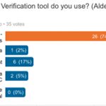
    I had no idea that there was a clock domain crossing (CDC) linkedIn group but indeed there is. Richard Brabant has set up a survey to see which tools people are using.


    The graph is somewhat confusing since, for example, Cadence Conformal is currently at zero but has a significant looking bar. But far and away the market leader (in this very limited “market”) is Atrenta’s SpyGlass product, with Real Intent a comfortable second.

    If you click over to the survey and vote then you can see the current numbers since the graph I have is presumably already out of date.

    Details of SpyGlass CDC, Atrenta’s clock domain crossing verification tool, are here (or click on the banner at the bottom).


    IC Custom IP Blocks – EM and IR Drop Effects

    IC Custom IP Blocks – EM and IR Drop Effects
    by Daniel Payne on 03-06-2012 at 5:33 pm

    Designing custom IP blocks is a challenge at the transistor-level and I wanted to learn what the recommended methodology and EDA tool flow was at Synopsys. They have a webinar that you can register for and it takes 30 minutes to learn what they have to say, or you can read a White Paper. If you cannot spare that much time, then my summary should answer some of your initial questions in about 10 minutes.
    Continue reading “IC Custom IP Blocks – EM and IR Drop Effects”


    Test Synopsys offensive in VIP and try the quiz

    Test Synopsys offensive in VIP and try the quiz
    by Eric Esteve on 03-06-2012 at 11:33 am

    I have recently blogged about Synopsys offensive in the Verification IP market. Did Synopsys again launched a new product, or announced a new acquisition? This would be a serious topic to blog, but today’s blog is closer to gaming than market analysis. Sometimes it’s good to have fun, even if the topic is serious! In fact, Synopsys has launched a quiz, the questions are centered about Verification and protocols: Ethernet, PCI Express, AXI4… I tried it, and I realized that I was certainly missing know how about these protocols… Do you want to check your VIP level of knowledge? Just go here!

    The above histogram is exhibiting a perfect Gaussian distribution, showing that the average player knows 50% of the right answer. Or, if you prefer, that half of the people who have tried the quiz have given a wrong answer once every two questions… If you plan to do this quiz, maybe you should review the protocol standards, listed in the picture below as well as the Discovery product brief. And keep in mind that the Discovery related questions have been created to highlight the advantages of the product (see my previous blog, or the list below), this may help you to correctly answer these questions.

    • Synopsys Discovery VIP speeds and simplifies verification of the most complex system-on-chip (SoC) designs.
    • Synopsys Discovery VIP offers greater performance, debug and coverage management features, ease-of-use and ease-of-integration for complex SoCs.
    • Synopsys Discovery VIP is written entirely in SystemVerilog, includes native support for UVM, VMM, and OVM, and is compatible with all related verification environments.
    • Synopsys Discovery VIP supports all major simulators.
    • Included with Discovery VIP, Protocol Analyzer enables engineers to quickly understand, identify and debug protocols in their designs.

    How did I score the quiz? That’s a very good question! To answer to it, I would say that I spend more time surfing the web for information, and blogging, than carefully reading the various protocol standard documentation. I hope it’s a fair answer!

    From Eric Esteve from IPnest


    Designing ARM Powered High Performance SoCs on 28nm and 20nm!

    Designing ARM Powered High Performance SoCs on 28nm and 20nm!
    by Daniel Nenni on 03-06-2012 at 9:17 am


    Last week I had an interesting meeting with GLOBALFOUNDRIES executives Kevin Meyer and Mojy Chian. It certainly seems that GFI has turned a corner! I will be in Dresden next week for DATE 2012 and will also visit the GFI Fab there. 28nm and 20nm are on track so expect an aggressive implementation plan from GFI this year.
    Continue reading “Designing ARM Powered High Performance SoCs on 28nm and 20nm!”


    OpenAccess DB – Productivity and Beyond!

    OpenAccess DB – Productivity and Beyond!
    by Pawan Fangaria on 03-05-2012 at 10:00 pm

    As I have been watching the developments in EDA and Semiconductor industry, it is apparent that we remain fragmented unless pushed to adopt a common standard mostly due to business reasons. Foundries are dictating on the rules to be followed by designs, thereby EDA tools incorporating them. Also, design companies needed to work with tools from different vendors. As a result various exchange formats appeared at various levels – layer, device, block, design and so on; first to define and satisfy the rule and second to exchange the information between different tools. Yet, the industry needed a common database for tighter integration and interoperability between various tools, eliminating data translation between formats. OpenAccess is an open standard database, owned and distributed by SI2 ; available at least after about 8-10 years of wait.

    There are multiple advantages of using OpenAccess database. I would not go into the details of its data exchange, capacity and performance benefits, but how it tremendously improves productivity in terms of design and tool development and robustness of the flow. SI2 provides database along with its access APIs; so any tool developed in-house or by 3[SUP]rd[/SUP] party on this database can be tightly integrated, thereby enabling a robust design flow based on multiple tools but working on the same database. This also eliminates multiple data translations through various formats which in turn eliminate unwanted errors and troubleshooting overheads. While talking to Brady Logan (Director of Business Development at SpringSoft), he showed me a demo of Laker environment. This reflects true use and advantage of OpenAccess.

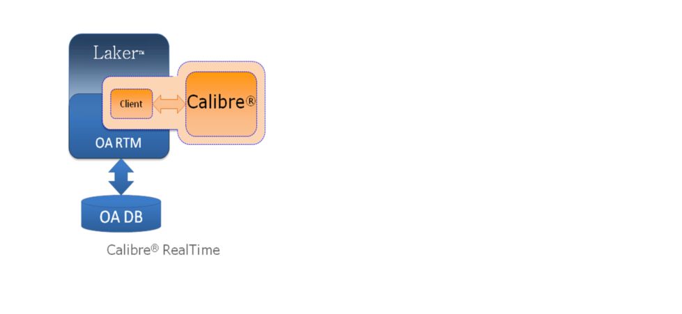
    The Laker (from SpringSoft) and Calibre (from Mentor Graphics) Realtime Runtime Model enables two tools to run concurrently on the same data base to provide users with real time sign off quality feedback on edits and DRC fixing. The use model’s elimination of Stream In and Stream Out has a proven 10X productivity gain over older methodology. Brady tells me that this use model has proven value at advance nodes where edits and fixes can create numerous violations of complex conditional rules. It’s obvious that all of the time consuming cycles through Stream during edit-verify-fix iterations go away.

    Overall flow in Laker system based on OpenAccess looks like this –

    Profitability – Imagine the amount of resources being spent by every company in maintaining every format and its translation to other formats and databases. Also, increase in design cycles due to formats. If all that expense can be saved, it will definitely increase in the bottom line of the whole industry as such and the resources can be deployed at other top-end challenges. OpenAccess enables saving that unnecessary cost. It must be noted that Cadence invested significantly in the making of this database though.

    Further Extensions – In one of my last article, I talked about design level analog constraints to be standardized. If OpenAccess database can be extended to include these constraints, then analog designs, even at the level of schematics and layouts can be shared with other parts of designs and tools from different vendors on the same database, thereby easing integration, edit and verification of the complete design together. Another good extension would be for 3D-IC to assimilate designs from various sources, specifically for information about TSVs, partitioning at different planes, power distribution networks and stress (thermal and mechanical) analysis; and tools for different usage working on the same database. For power distribution, CPF (Common Power Format) and UPF (Unified Power Format) formats are available, but they need to be unified in a single format first for greater interoperability.


    By Pawan Kumar Fangaria
    EDA/Semiconductor professional and Business consultant
    Email:Pawan_fangaria@yahoo.com