Bronco Webinar 800x100 1

CDNLive: the Keynotes

CDNLive: the Keynotes
by Paul McLellan on 03-13-2012 at 2:24 pm

There were three keynotes at CDNLive this morning, and one theme ran through them: collaboration. In fact there was one specific instance of collaboration that all three people mentioned. Taping out an ARM Cortex-A15 in TSMC 20nm technology using a Cadence tool flow.

Lip-Bu, Cadence’s CEO, went first. He had some numbers showing that semiconductors and electronics should continue to grow at twice the rate of world GDP. And the GSA semiconductor index is all going up for the next couple of quarters. Underlying this growth is that increasing integration leads to many more devices. Mainframes shipped perhaps 1M units. PCs 100M units. But mobile internet (smartphone, iPad) are in the 10B unit range.

Rick Cassidy of TSMC was next up. He had an interesting retrospective on cost. From 1970 to today, transistor cost has reduced by 10[SUP]-8[/SUP] and microprocessor cost per transistor per cycle by 10[SUP]-11[/SUP]. An example Rick uses with MBA students (who know nothing about semiconductor) is that if Manhattan was a chip in 1962, by today it has shrunk so much that it fits in an iPod screen. And if we continue on the same path for another 50 years, the entire world will fit in that screen. Of course driving this is the scale of fabs like those TSMC is building. 180,000 12″ wafers per month. Last year, TSMC shipped 13.2M 8″ equivalent wafers. That’s a lot of silicon.

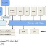
Tom Lantzsch of ARM started by asking everyone whether they were more likely to return home if they had forgotten their wallet than their phone and most of us figured we could do more easily without our wallet. His interesting statistic of the day is that there is a need for approximately one server in the cloud for every 600 mobile phones (and, for every 120 or so tablets). ARM is increasingly moving into the home (smartTV) and the car (infotainment). Underlying everything ARM does is energy efficiency (aka low power). This is why ARM is moving into servers in a move that has many commentators perplexed. ARM’s view is that servers will mimic what has happened in SoCs in smartphones, with a general purpose CPU (Intel) being replaced by multiple smaller CPUs and specialized functions such as video decode (of course, no prizes for guessing which CPUs Tom is expecting those to be). Developing countries simply don’t have the power to build a datacenter the way they are currently done. Instead, he expects servers with a power budget of 5W such as the Calxeda one, simplifying not just power, but cabling and physical size. Servers are likely to be specialized since, for example, netflix doesn’t need general purpose servers, just specialized video pumps.

Tom’s equivalent of TSMC’s wafer statistics were that ARM now has 275+ silicon partners, 900+ ecosystem partners, 30B+ ARM-based chips shipped. 50+ mobile phone application processors. 100+ phone designs. 100+ tablet designs (where are they all?), 1B+ applications. That’s a lot of compute power.


The Coming Gamer Tablet from…… Apple!

The Coming Gamer Tablet from…… Apple!
by Ed McKernan on 03-13-2012 at 11:25 am

After the introduction of the NEWiPAD, Apple has placed itself just two short steps away from dominating the computer market – including PCs. One step, which is widely reported, is a smaller iPAD with an 8” screen that aims for a $299 price point. Amazon will take the rest of the market under $299. The second step is purely speculation on my part but is within easy reach of the current hardware and will result in re-alignments in the semiconductor industry to the benefit of Apple and detriment of everyone else. A leveling will occur that forces some to return to their area of expertise, including a software company based in Redmond. The strategy is multi-faceted and thus will require an additional blog to fully outline.

To begin with we must recognize that the NewiPAD will not only reinforce but expand Apple’s lead in the tablet market. Tim Bajarin in his latest tech opinions column calls it revolutionary because of the impact the high-resolution screen will have on several industries. It is a great article that I highly recommend to anyone who follows the computer industry. After reading this, I sensed that Apple will not want to stop with what they have in the current iPAD but extend it further in order to make it even more competitive with respect to ultrabooks.

As a long time processor marketing guy, I see an opportunity for Apple to go one step further and that is to leverage the Retina display with a high performance graphics solution connected to its future A6 processor. For an additional $20-$25 of BOM cost, Apple can add an AMD or nVidia mobile graphics chip that will push the iPAD into a similar performance window as the ultrabooks to be powered by Intel’s Ivy Bridge – ULV parts. That’s because in this tablet, ultrabook market the Processor is not required to be high performance as the work-load shifts to the graphics unit. Thus the decision by Intel to spend the new transistor budget on improving the Ivy Bridge graphics unit.

The interesting dynamic that will play out in 2012 is that Intel’s Ivy Bridge ULV part will probably not drop below $225 for PC OEMs. Apple therefore will have the opportunity to introduce a $899-$999 Gamer iPAD with 4G LTE that has a $175 processor+graphics cost advantage. Furthermore, I can envision a Gamer iPAD with an 11” screen (same as MAC Air PC) that with an optional keyboard can find its way into the corporate market as an alternative to a Windows 8 machine running on an ARM based nVidia Tegra 3 or an Intel x86 based Atom processor. Apple then will leave it up to corporations to decide if they need an Intel Ivy Bridge based MAC Air or an A6 ARM based iPAD with PC level graphics selling at a discount but delivering higher margins to Apple.

In my previous blog, I mentioned how Apple’s Phil Schiller, Senior VP or Worldwide Marketing, stated that the new A5X processor with quad core graphics was 4 times faster than nVidia’s Tegra 3 and that nVidia resisted responding aggressively to the claims because they had other business at risk with Apple. The de-positioning of the Tegra 3 was a deliberate attempt by Apple to say to nVidia that they should abandon their tablet and smartphone attempts and return to their core, which is developing high-performance PC and supercomputing graphics solutions (In addition, Apple has effectively tagged competitive tablets as less than devices). With a Gamer Tablet, Apple will in effect force nVidia to choose between competing with them or cooperating, because the alternative is to let AMD take the business.

In the next blog we can look at Apple’s likely impact on Intel and Qualcomm in the coming year.

Full Disclosure: I am Long AAPL, INTC, QCOM and ALTR


More Growth in EDA

More Growth in EDA
by Daniel Payne on 03-12-2012 at 6:53 pm

I love to read good news about growth in EDA especially when our industry has seen single-digit growth for several years now. What I read on March 8th from ClioSoft stated a 53% increase in bookings for 2011, now that’s what I call growth.

ClioSoft provides Hardware Configuration Management (HCM) software to EDA users typically doing transistor-level IC design for both schematics and layout. I’ve been able to speak with several users of ClioSoft tools last year to find out first-hand what their experience was in adopting and using HCM in an IC design flow:

I blogged recently about, “What Just Changed on my Transistor-Level Schematic” and it’s getting plenty of discussion both here at SemiWiki and on LinkedIn with some 1,261 page views at SemiWiki in under a month. Engineers are interested in how to manage their IC design projects better, especially as their team size grows and becomes geographically separated.

Also Read

What Changed On My Transistor-Level Schematic?

Manage Your Cadence Virtuoso Libraries, PDKs & Design IPs (Webinar)

EDA Tool Flow at MoSys Plus Design Data Management


Virtual Prototype your SoC including FlexNoC

Virtual Prototype your SoC including FlexNoC
by Eric Esteve on 03-12-2012 at 1:10 pm

Designing larger than ever SoC, integrating multiple ARM’s Cortex-A15 and Cortex-A9 microprocessor cores as well as complexes IP functions like HDMI controller, DDR3 Memory controller, Ethernet, SATA or PCI Express controller are pushing designers to search for better price, performance and area tradeoffs and the SoC interconnect plays a vital role in serving this need. Using an advanced Network-on-Chip (NoC) like Arteris FlexNoC is an efficient solution to optimize the SoC and get the best possible return on the high investment linked with state of the art SoC development, by launching the IC in the right market window and benefit from a TTM advantage over the competition. Architects also want to virtually prototype their design, as it can be a good way to run these price, performance and area tradeoffs at early stages of the design, that they can do using Carbon’s SoCDesigner Plus, and prove their design assumptions before committing to the design implementation.

The joint Carbon/Arteris solution offers design teams a way to easily create and import accurate Arteris FlexNoC interconnect models for Carbon SoCDesigner Plus: the new Carbon/Arteris flow allows Carbon’s SoCDesigner Plus users to use Arteris FlexNoC to configure their NoC interconnect fabric IP and then upload the configuration to Carbon IP Exchange. The web portal then creates a 100% accurate virtual model of the configuration and makes it available for download and use in SoCDesigner Plus. “We see strong demand for models of Arteris’ NoC interconnect IP,” states Bill Neifert, chief technology officer at Carbon Design Systems®, the leading supplier of virtual platform and secure model solutions. “Our partnership with Arteris enables engineers to make architectural decisions and design tradeoffs based upon a 100%-accurate virtual representation.”

“Simulation with virtual models of our NoC interconnect IP are the best way to make system-on-chip architectural optimizations and tradeoffs,” comments Kurt Shuler, Arteris’ vice president of marketing. “By partnering with Carbon to make 100% accurate models of our IP available on Carbon IP Exchange, we are empowering design teams to utilize virtual models earlier in the design process.”

Going on Carbon IP Exchange web portal, we can see that the partnership allow to run a secured flow: the FlexNoC model is compiled directly from Arteris’s register transfer level (RTL) code and maintains 100% functional accuracy. The model integrates directly with Carbon’s SoC Designer Plus virtual platform. There is no “interpretation”, no modeling task in between the RTL source code from Arteris and the virtual prototyping usage within Carbon SoCDesigner Plus.

To learn more about FlexNoC IP from Arteris availability in IP Exchange web portal from Carbon design Systems, just go here.

By Eric Esteve from IPNEST


Book Review – iWoz

Book Review – iWoz
by Daniel Payne on 03-12-2012 at 11:01 am

I bought my first personal computer in 1979, it was a Radio Shack TRS-80 Model I with just 16KB of RAM, a BW monitor and casette tape for storage. The reason that I chose the Radio Shack over the Apple II was that it cost less, so I was always interested in Apple products and the engineers behind them since the early days. It was pure delight to read the autobiography of Steve Wozniak called iWoz, and the Kindle version costs only $8.61.

Wozniak writes in a style that sounds like he is having a conversation with you, face to face, very readable and personal. In the book he covers his family, upbringing, school days, pranks and how his father’s job in engineering attracted him to also pursue an engineering career.

A fascination with science, math and building electronics projects set the stage for Steve Wozniak to meet the younger Steve Jobs and together they start building and selling illegal phone devices to make toll-free calls anywhere in the world. Wozniak does stints in college at Colorado and California, then lands a dream job at HP where he loves working on calculator designs. Part-time outside of HP he designs and builds the Apple I and Jobs sells the first 100 to a store for $50,000 to start their fledgling company.

In those early days an engineer like Wozniak would first design the computer system on paper, then breadboard the design with wire wrap, plug in chips, then start debugging it by using oscilloscopes or simply connecting the output to a TV. Very little software existed to simulate an actual design, so it was build first, then debug in hardware.

Wozniak hesitantly leaves HP to found Apple and the folks at HP simply let him go. They forgot to copyright the Apple 1 and soon there was an exact clone, so for the Apple II they didn’t repeat that mistake. Engineering won out over marketing (Jobs) in the Apple II as Wozniak insisted that they give seven expansions slots, not just a measly two. It was interesting to read about how DRAM chips from Intel replaced SRAM in the Apple computer, how they choose their CPU, writing a dialect of BASIC, interfacing with the first 5 1/4 inch floppy drives, creating boot ROMs, etc. If you are a computer geek, then this story is for you.

The rate of growth of Apple and how its IPO made hundreds of millionaires is the stuff that drives risk takers of all sizes in Silicon Valley and around the world to build their own companies and try to change the world.

After the IPO at Apple Wozniak had a plane crash, recovered and then started to move in a different direction – like finishing up his fourth year of college under an assumed name, sponsor rock concerts and promote peace between the US and the Soviet Union.

Fame and fortune took a personal toll as Wozniak got divorced and then re-married. He talks about helping out his local school district by teaching a computer class, then venturing into charities and even funding the Tech Museum in San Jose.

In the 1980’s I can remember visiting Apple Computer to sell them EDA software at a time when they were still designing their own graphics chips. When Steve Jobs saw the GUI on our EDA tool he said, “Well, that’s just brain dead.” Of course, he was right and now that EDA company is history.

If you are curious about the history of the Personal Computer and want to hear it straight from the engineer of the Apple I and Apple II, then get this book and enjoy the journey.


My Design Automation and Test in Europe Conference Agenda (DATE 2012)

My Design Automation and Test in Europe Conference Agenda (DATE 2012)
by Daniel Nenni on 03-11-2012 at 7:00 pm


As this blog is being posted I’m on my way to Dresden for the 2012 Design Automation and Test Conference. DATE used to bounce between Munich and Paris, I have attended many times but not in the past couple of years. No excuse really, just busy with other things.
DATE 2012 Highlights in Dresden include E-Mobility and More-than-Moore in the Conference and Ecosystem Exhibition. For me DATE 2012 holds three exciting things:
Continue reading “My Design Automation and Test in Europe Conference Agenda (DATE 2012)”


Power Issues for Chip and Board: webinar

Power Issues for Chip and Board: webinar
by Paul McLellan on 03-10-2012 at 4:24 pm

Last month Brian Bailey at EDN moderated an interesting webinar about power issues. Unusually, it combined two different domains: doing things by modeling and actually taking measurements off real chips and boards. The two participants were Arvind Shanmugavel from the Apache subsidiary of Ansys, and Randy White from Tektronix.

Nobody needs me to tell them that power is a major issue for chip and board design. This webinar wasn’t so much about how to reduce power, important though that is, but more about how to deliver power and analyze what is being delivered, and then take measurements to see what is really happening. With low noise margins but a transistor threshold voltage that cannot change much, issues with the power supply such as voltage droop will cause systems to fail.

One of the biggest areas is active state power management whereby the software works with the underlying chip to control things like voltage island and power down blocks. If a block doesn’t need to produce its result fast then why bother to run it in high speed/high power mode. The challenge with this is that the transitions, changing the voltage of a block or powering it on or off produce major transients in the power network. The most extreme is power up a block that was powered down. Done naively the inrush current will cause the voltage to drop to the whole chip and so the received wisdom is to power the block up slowly (which, of course, means you know far enough in advance that you’ll need it) and only connect the main power transistors when the block is up to the supply voltage (so no inrush current).

For me the most interesting parts were Randy’s comments about measuring everything since it’s not an area I know lots about (I’m a software guy by background). At GHz performance levels, everything affects everything. Every probe has its own inductance, capacitance, resistance and so affects the measurement. I had no idea that Tektronix provides Spice models of all their probes so that you can work out what you expect to see on the scope given which probes you are using, since it differs from what the simulation says the actual signal value will be.

Arvind had an interesting example showing how the thermal map of a die varies dependent on the package. And not just due to thermal aspects of the package but transient power supply effects too.

We used to have a lot of margin on power supplies, with as much as 25% of tolerance. Now, especially in battery powered mobile devices it can be as low as 5%. This requires both an accurate power model and accurate ways of taking measurements off the actual devices without, Heisenberg style, perturbing the actual system too much.

The webinar is here.


Common Platform Technology Forum: Peering into the Future

Common Platform Technology Forum: Peering into the Future
by Paul McLellan on 03-10-2012 at 9:00 am

Next Wednesday is the Common Platform Technology Forum. “Common Platform” is a name that only a committee could have come up with, giving no clue as to what it actually is. As you probably know, there are various process clubs sharing the costs of technology development (TD) and one of them consists of IBM, Samsung and Global Foundries. Although they have many partners, historically they have worked closely with ARM and Synopsys.

TD versus capital has gone through a couple of phases. It used to be that anyone could build a fab but getting a process to run in it was expensive. Then in the 90s, fabs suddenly became really expensive and the cost of licensing a process was a lot less. But then TD got really hard again, and it became so expensive that only Intel could really afford to go it completely alone. Hence alliances like the Common Platform.

Wednesday March 14th at the Santa Clara Convention Center is this years Common Platform Technology Forum. The keynote speakers (from 9am to 11.30am) are:

  • Dr. Gary Patton, Vice President of Semiconductor Research & Development Center, IBM
  • Gregg Bartlett, Chief Technology Officer, GLOBALFOUNDRIES
  • Dr. Jong Shik Yoon, Senior Vice President of Semiconductor R&D, Samsung
  • Simon Segars, Executive Vice President and General Manager, Physical IP Division, ARM

There is a partner pavilion then open for the rest of the day. I’m presuming lunch is provided there too. And since it is Pi day (3.14), from 1.30pm they will be serving…wait for it…specialty pies.

From 1-2pm is a panel session on the R&D pipeline for future technology innovation. There are representatives of (surprise) Global Foundries, Samsung and IBM. Along with ARM and the College of Nanoscale Science and Engineering (which I confess to never having heard of).

In the afternoon are presentations from Synopsys, Cadence and Mentor (how’s that for EDA neutrality?).

At 2pm, John Chilton of Synopsys talks about designing ARM-based SoCs at 28nm and 20nm. He is followed, at 3pm, by Sampta Bansal of Cadence, who sees Synopsys’s 20nm and raises it by talking about delivering on 20nm and embarking on 14nm. Then, at 4pm, Mentor’s Michael White talks about double patterning at 20nm.

For me the Mentor presentation looks the most interesting since it looks like a sort of introduction to double patterning, a subject that I need to learn a lot more about. And so, probably, do you. To register click on the banner below.


Elpida and Japan Inc

Elpida and Japan Inc
by Paul McLellan on 03-09-2012 at 2:17 pm

Last week, the Japanese memory company Elpida filed for bankruptcy. There is worldwide overcapacity in DRAM and somebody had to go. Its strength and the weakness was that it was much more outward facing than most of the Japanese semiconductor and electronic industry. So it had to compete globally and wasn’t up to the task.

I think looking at the Japanese mobile phone industry is revealing. If you visit Japan you get some idea of the problem. Everything is too inward looking. All the mobile phones are great and seem in some ways to be ahead of what we have in the US, and they are all made by Japanese manufacturers. But that is the problem, they are made by manufacturers who have given up in the rest of the world.

Greg Hinckley, the COO of Mentor Graphics, once told me about interviewing a candidate for a finance position who came from American Airlines. Their focus, the candidate said, was to touch down 30 seconds ahead of United. It was as if Southwest and Jet Blue and all the rest didn’t even exist. Being the best airline just meant being the best legacy airline: beat United, Delta and the others.

The Japanese cell-phone companies are like that. They are so competitive for their share of the Japanese market that they have given up on the global market and what it takes to compete there. Of course, the Japanese cell-phone transmission standards are different which means that you have to decide whether to compete in Japan, overseas or both. Those different standards may have looked like a giving a good unfair advantage to the Japanese since Nokia, Ericsson or Samsung were unlikely to focus on the Japanese standard first even during the initial high-growth period. But on the other hand the Japanese manufacturers have no market share in the rest of the world, which is orders of magnitude bigger.

Last time I visited the usual Japanese semiconductor companies I got the feeling that they were all only competing with each other. By and large they were making chips to go into consumer electronics products for the Japanese market. There were obviously far more products and far more chips being done than could possibly make money, just like all those cell-phones and cell-phone chips couldn’t be making money (not to mention that the Japanese market is already saturated).

With too many companies, and too many uncompetitive semiconductor divisions, consolidation is to be expected. But Japanese politics is inward facing too and so they can only merge with each other and gradually move towards what I call Japan Inc in the semiconductor world (to be fair, this same issue is one that affects my American Airlines example; British Airways or Lufthansa is simply not allowed to buy a major stake, recapitalize them and clean them up because congress has laws preventing it).

I said a couple of years ago: “So it looks like gradually the semiconductor companies will consolidate into a memory company (Elpida) and a logic company and, based on past history, they won’t take the hard decisions necessary to be competitive globally rather than just in Japan.”

Well, it didn’t work out too well in memory, although presumably Elpida will re-emerge in some form.

On the logic side, NEC/Renasas(Hitachi/Mitsubishi), Fujutsu and Panasonic are rumored to be in discussions to merge. Toshiba is not on the list since it seems to be strong enough to go it alone, at least for now. But as fabs get bigger, and the cost of an individual design gets bigger, you can only make money addressing large global markets, not supplying a fragmented domestic market. Based on past form, merging Mitsubishi and Hitachi to form Renasas, and before they had finished getting that sorted out, adding them into NEC, and before that was done throwing in Fujitsu and Panasonic…let’s come back in a year or two and see how that’s working.

I guess I’ll stick with my statement from a couple of years ago. It’s still looking good.


Apple’s New iPAD and the End of PC Benchmarks

Apple’s New iPAD and the End of PC Benchmarks
by Ed McKernan on 03-09-2012 at 10:19 am

With the introduction of the “New iPAD”, we now have the 2012 benchmark for the tablet market, including the offerings that will come from Amazon later in the year. As has been noted earlier, with each new mobile product iteration Apple unmoors itself from the PC foundations of Microsoft, Intel and even nVidia and AMD. At the unveiling of the new iPAD, Apple spent very little time extolling its wonderful, new A5X CPU and instead played up the experiences possible with their high definition Retina Display and high-speed 4G LTE communications. The number of ARM cores, the speed of the processors, the graphics engines are all of lesser concern than what the consumer experiences with the New iPAD connected to the Apple Ecosystem.

Back in the mid 1990s, when the world was trained to measure the value of their PC with the simple three letters: M-H-z and Intel was able to build an empire by delivering a new chip at a cadence of every 2 months backed by a full suite of synthetic benchmarks, there was the beginnings of an alternative vision of the future. The internet was just beginning to take off and just as significant, the bandwidth and wireless revolution that was well articulated by George Gilder in his book Telecosm pointed to a time in the future when the processor’s value would decrease relative to that of the communications infrastructure. Qualcomm was one company that Gilder tracked closely and looking back now almost 20 years later we can say it was his most prophetic selection.

Overlooked by nearly everyone in the 1990s was the importance and rise of the role of the graphics processor. Jen Hsun Huang’s vision of the future where the graphics processor becomes more important than the x86 processor was correct as can be seen in the increased die area dedicated to graphics within Intel’s Ivy Bridge and AMD’s APU offerings. After 4 cores, is there any value in an additional x86 CPU? The data says no. Intel’s transition from Sandy Bridge to Ivy Bridge is all about a vastly expanded graphics chip that for once challenges nVidia. As with processors, the graphics vendors measured their greatness with a full suite of benchmarks, which are now going to be cast into irrelevance in the new mobile markets with the New iPAD as the standard bearer. And soon to be followed by the iPhone 5 and a smaller $299 Retina display based iPAD in the fall. Did I mention the awesome Retina Display?

Because Apple is the leader in the mobile industry it is given great regard as to what is significant and supposedly true. When Apple’s Phil Schiller, Senior VP of Worldwide Marketing, displayed a graph that showed the new A5X with its quad core graphics is 4 times faster than the Tegra 3 without showing a benchmark, no one begged to question him. It is now written in hundreds of articles and plastered over the Apple web site. Personally, I am sure the Tegra 3 stacks up well to the A5X.

On the day after the launch, the technical web site Tom’s Hardware asked nVidia if it was true that the A5X was 4 times faster than Tegra 3. The response was telling in that nVidia wasn’t willing to challenge Apple’s claim on benchmarks without hardware to test. Should nVidia find out in the coming weeks that the Tegra 3 is indeed on a par or better than the A5X, I doubt that they will make it public. To do so would jeopardize their attempts to win the next generation MacBook Pro graphics sockets. And so they face a dilemma of losing their benchmark marketing tools in order to remain a supplier. Apple has effectively de-positioned nVidia’s Tegra 3 that is slated to be in a number of Android based tablets and smartphones this year. The Tegra 3 was smothered in the cradle. Qualcomm and Intel will be the benefactors of this deliberate Apple Branding slight of hand.

As I wrap up this blog posting, TI has just reported that sales will come in less than previous guidance based on slowing OMAP sales. In addition there are reports that Broadcom is challenging TI for the sockets for the next Amazon Kindle. Combine this with Intel’s aggressive push into ZTE, Lava, Orange, Lenovo and Motorola and one gets a picture of a fast commoditizing application processor and graphics market. The one chip inside the mobile smartphone and tablet that demonstrates high value is the baseband chip, which is being dominated by Qualcomm as they start to ramp 4G. Intel knows this and has a massive R&D effort underway to catch them in time for the launch of Haswell based ultrabook platforms in 2013.

Recent remarks by Intel executives appear to support the position that Intel would gladly torch the market with which the Atom Medfield processor is designed to serve in order to eliminate nVidia, Broadcom, TI, Marvell and AMD as viable competitors and more importantly to increase the data center footprint that spits out an unbelievable 50% operating margins. Qualcomm and Intel share a common goal of ramping 4G LTE into mainstream price points so that the Mobile Bandwidth Tsunami causes profits to rain down on the two ends of the wireless network.

The Era of Benchmarks is Coming to an End or I should say the new mobile market has tossed aside the benchmarks with which the PC market operated under for the last 20 years. I expect the Ultrabook PCs due out this year with their Retina based touch screeens and extended battery life to follow the pattern set by smartphones and tablets. The semiconductor playing field continues to experience rapid and dramatic change.

Full Disclosure: I am Long AAPL, QCOM, INTC, and ALTR