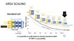
A comprehensive report from the US Department of Energy (DOE), “Semiconductor Supply Chain Deep Dive Assessment” (February 2022) calls for a 1000X energy efficiency improvement that is required to maintain future compute requirement needs given a finite amount of world energy production. Energy efficiency is at the top of designers’ minds today. A holistic approach to energy efficiency must start at the earliest stages of the design flow, at the architectural and micro-architectural levels. It is at those levels of abstraction where designers can evaluate power-performance-area tradeoffs and create energy-efficient architectures. Later stages in the design process present limited opportunities for power reduction.
Energy efficiency and power optimization efforts must be guided by power analysis at all levels of abstraction. Early power analysis is intrinsically less accurate than signoff power analysis in the implementation phases, but the goal of early power analysis must be to provide consistent accuracy to the designers to enable them to make informed decisions.
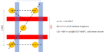
Traditional Register Transfer Level (RTL) power analysis tools take into account a very limited amount of information related to the actual implementation of the design. Fast synthesis technologies used in such tools are typically not timing driven, have limited parasitic capacitance estimation capabilities, build simple fanout-driven clock tree structures, and use imprecise heuristic methods for glitch power calculation.
These considerations call for the new generation of RTL power analysis tools to provide consistent accuracy by leveraging technology-related information, timing constraints, and accurate glitch power modeling. Such tools deliver a tight correlation of RTL power analysis vs. final signoff analysis in a consistent manner. This consistent accuracy is made possible only with the deep understanding of the implementation and signoff power calculation algorithms.
If you are designing chips for high-performance computing (HPC) and data center applications, bandwidth is, of course, a key consideration. However, as data centers get bigger and the required compute power increases, keeping power consumption to a minimum becomes a priority. In addition to power, latency is another key concern for HPC and data center SoC designers as access to the available memory pool is becoming a bottleneck and must be allowed in nanoseconds.
Webinar: Achieving Consistent RTL Power Accuracy
Register Transfer Level (RTL) power analysis, performed early in the design cycle, is a key component of end-to-end methodology to maximize energy efficiency. Such analysis has become a critical requirement for many IC designs today and in the future. Although RTL power analysis technology has been available to designers for many years, traditional approaches have relied on heuristic methods – thus lacking consistent accuracy. This webinar, presented by Alexander Wakefield, Synopsys Scientist, will focus on Synopsys RTL power analysis technology and best practices that achieve consistent accuracy in the design flow.
First, the motivation for RTL power analysis will be briefly outlined in the context of the overall methodology. Next, the basics of power consumption and associated calculations will be reviewed. Following that, several key factors affecting RTL power accuracy will be examined: fast synthesis and mapping, clock tree modeling, and parasitics estimation. These factors will also be compared with heuristic methods, and finally, some of the best practices to achieve good correlation and consistent accuracy will be covered.
REGISTER HERE
Presenter Bio:
Alex Wakefield is a Synopsys Scientist, with degrees in Engineering and Computer Science from the University of Adelaide, Australia. He has worked for more than 20 years in many areas including Synthesis, Simulation, SystemVerilog, UVM, Constraints, Coverage closure, and Embedded-Software. He has presented papers at many conferences and holds multiple patents. The last few years Alex has primarily been focused Power-Estimation, Leading the Synopsys global rollout of Power-Estimation with Zebu. He is involved in all Synopsys Power-Estimation engagements worldwide.
Also Read:
Synopsys Crosses $5 Billion Milestone!
Configurable Processors. The Why and How
New ECO Product – Synopsys PrimeClosure
UCIe Specification Streamlines Multi-Die System Design with Chiplets