
As digital transmission speeds increase, designers use various techniques to improve the signal-to-noise ratio at the receiver output. One such technique is the Decision Feedback Equalizer (DFE) scheme, commonly used in high-speed Serializer-Deserializer (SerDes) circuits to mitigate the effects of channel noise and distortion. The DFE scheme relies on decisions about the levels of previous symbols (high/low) to correct the current symbol. This allows the DFE to account for distortion in the current symbol that is caused by the previous symbols.
However, DFE error propagation can occur when feedback signals are incorrect. Following are some of the situations that contribute to DFE error propagation. DFE circuits operate by using feedback to equalize the received signal, but this feedback can also amplify noise and distortion in the signal. In some cases, the feedback can overemphasize certain frequencies, leading to an increase in noise at those frequencies and an increase in the Bit Error Rate (BER). The mechanism also relies on accurate timing to make decisions about the incoming data. If there are timing errors in the feedback loop, these errors can propagate and cause additional errors in the received data. Nonlinear distortion in the transmission channel can also cause DFE circuits to make incorrect decisions about the received data. These errors can then propagate through the feedback loop and cause additional errors in the data. As the DFE scheme makes decisions based on previous decisions, errors in the feedback loop accumulate over time.
As noted above, DFE error propagation can lead to increased BER and reduced signal integrity. Increased BER in turn leads to data errors and reduced system performance. Reduced signal integrity results in increased jitter and reduced eye height, leading to errors in data transmission. As a result, DFE error propagation can significantly impact the performance of high-speed SerDes circuits and must be carefully managed to ensure reliable data transmission.
But existing statistical simulation methods cannot properly consider DFE feedback, and time-domain simulations become impractical for low error probabilities. A whitepaper by Siemens EDA presents a statistical solver that can find bit error ratio or symbol error ratio in the presence of isolated and burst DFE errors. The solver can accurately consider transmit and receive jitter, crosstalk aggressors, noise, and other impairments, and is useful in choosing forward error correction (FEC) schemes and parameters. The paper defines the essential building blocks of the statistical solver, including the main elements of statistical analysis, the convolution term for DFE feedback, the symbol error probability matrix, and the flow to find BER/SER metrics. It also discusses the use of a modified iteration process to find the probability distribution of symbol error groups and presents experimental results of the statistical solver.
The following are some excerpts from the whitepaper.
Building statistical eye that includes DFE errors
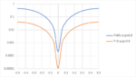
The method is considered a Markov chain with a transition operator defined by a function that transforms known error probabilities into new error matrices measured from the eye diagram. The process involves building a statistical eye diagram from which error probabilities are calculated. The iterations continue until the error probability matrices become equal up to machine precision. The iterations are consistent and converge to the same solution regardless of initial settings. Two examples are given to illustrate the convergence of the iterations with statistical solver in the loop. The first example is the simulation of a 200GBASE-CR4 link, while the second is the CEI VSR channel with 4 taps DFE.
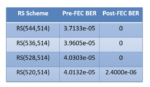
Choosing FEC parameters
The size of FEC needed to correct the error groups can be determined by analyzing the probability parameters distribution of error groups found from statistical simulation.
The simulations with FEC demonstrate the importance of knowing the burst error distributions for the proper choice of FEC parameters while keeping the FEC-induced latency to a minimum. The statistical analysis results can be relied upon for the purpose of FEC parameter optimization for a large variety of channels.
Summary
The whitepaper presents a novel statistical simulation method that considers the effect of DFE error propagation in SerDes links. Simulation speeds are sufficient to make this approach a routine part of the design process that require multiple channel compliance evaluations and FEC parameter optimization. You can download the entire whitepaper from here.
Also Read:
Hardware Root of Trust for Automotive Safety


