You are currently viewing SemiWiki as a guest which gives you limited access to the site. To view blog comments and experience other SemiWiki features you must be a registered member. Registration is fast, simple, and absolutely free so please, join our community today!
Memories have always played a critical role, both in pushing the envelope on the semiconductor process development front and supporting the varied requirements of different applications and use-cases. The list of the various types of memories in use today runs long. At a gross level, we can classify memories into volatile or non-volatile, read-only or read-write, static or dynamic, etc. And when it comes to the cost, performance, power and area/form factor of an electronic system, a lot rides on the use of all the right memories for the application. The lion’s share of the attention is paid to the effective use of Static Random Access Memories (SRAMs) and Dynamic Random Access Memories (DRAMs) as per the tradeoff benefits to be derived. While the need for higher density memories that consume very low power and perform like SRAMs has always been there, applications were able to manage with a judicious mix of DRAMs and SRAMs.
But over the recent years, fast growing markets such as modem, edge connectivity and EdgeAI have started demanding more from memories. Additionally, with the rise of the Smart Internet of Things (IoT) and wearable technology, there is an increasing demand for memory solutions that can provide high performance and low power consumption to extend battery life. These applications want memories that deliver the performance and power benefits of SRAMs (over DRAMs) and the density and cost benefits of DRAMs (over SRAMs) rolled into one. Fortunately, such a type of memory was invented quite a while ago and is called the Pseudo Static Random Access memory (PSRAM). PSRAM manufacturers were waiting in the wings for adoption drivers such as the above mentioned fast growing applications. The list of PSRAM memory suppliers includes AP Memory, Infineon, Micron Technology, Winbond Technology, and others.
What is PSRAM? [Source: JEDEC.org]
(1) A combinational form of a dynamic RAM that incorporates various refresh and control circuits on-chip (e.g., refresh address counter and multiplexer, interval timer, arbiter). These circuits allow the PSRAM operating characteristics to closely resemble those of a SRAM.
(2) A random-access memory whose internal structure is a dynamic memory with refresh control signals generated internally, in the standby mode, so that it can mimic the function of a static memory.
(3) PSRAMs have nonmultiplexed address lines and pinouts similar to SRAMs.
Mobiveil
Mobiveil is a fast-growing technology company that specializes in the development of Silicon Intellectual Properties, platforms and solutions for various fast growing markets. Its strategy is to grow with fast burgeoning markets by offering its customers valuable IPs that are easy to integrate into SoCs. One such IP is Mobiveil’s PSRAM Controller which has been in mass production for more than half-a-decade with customers across the US, Europe, Israel and China. The controller is available in different system bus flavors such as AXI and AHB and supports a variety of PSRAM and HyperRAM devices from many suppliers. The company recently expanded the list with the addition of support for AP Memory’s latest 250MHz PSRAM devices.
AP Memory
AP Memory is a world leader in PSRAM and has shipped more than six-billion PSRAM devices to date. The company has positioned itself as a market leader in PSRAM devices, providing a complete product line of high-quality memory solutions to support IoT and wearables market segments. The company continuously launches competitive products and provides customized memory solutions based on customer requirements.
Mobiveil-AP Memory Partnership
This partnership expects to bring significant benefits for SoCs, as PSRAM devices offer 10x higher density over eSRAM, 10x lower power compared to standard DRAM, and close to 3x fewer pin count. These advantages will result in lower power consumption, higher performance, and cost savings for the systems that leverage PSRAMs.
The result of the partnership is a controller IP that will provide cost-effective, ultra-low-power memory solutions for system designers. Mobiveil has adapted its PSRAM Controller to interface with AP Memory’s new PSRAM device that goes up to 250 MHz in speed and densities from 64Mb to 512Mb, supporting x8/x16 modes. This integration will allow SoC designers to take advantage of the high performance of the PSRAM controller at very low power, making it ideal for battery-operated applications, and extending the standby time of devices.
The PSRAM controller supports Octal Serial Peripheral Interface (Xccela standard), enabling speeds of up to 1,000 Mbytes/s for a 16-pin SPI option. Additionally, it provides support for a direct memory mapped system interface, automatic page boundary handling, linear/wrap/continuous/hybrid/burst support, and low power features like deep and half power down.
Mobiveil’s flexible business models, strong industry presence through strategic alliances and key partnerships, dedicated integration support, and engineering development centers located in Milpitas, CA, Chennai, Bangalore, Hyderabad and Rajkot, India, and sales offices and representatives located worldwide, have added tremendous value to customers in executing their product goals within budget and on time. To learn more, visit www.mobiveil.com.
There were quite a few announcements at the TSMC Technical Symposium last week but the most important, in my opinion, were based on TSMC N3 tape-outs. Not only is N3 the leading 3nm process it is the only one in mass production which is why all of the top tier semiconductor companies are using it. TSMC N3 will be the most successful node in the history of the TSMC FinFET family, absolutely.
(Graphic: TSMC)
In order to tape-out to 3nm you need IP and high speed SerDes IP is critical for HPC applications such as AI which is now the big semiconductor driver for leading edge silicon. Enabling chiplets at 3nm is also a big deal and that is the focus of this well worded announcement:
Successful launch of 3nm connectivity silicon brings chiplet-enabled custom silicon platforms to the forefront Alphawave Semi 3nm Eye Diagram
(Graphic: Business Wire)
LONDON, United Kingdom, and TORONTO, Canada – April 25, 2023 – Alphawave Semi (LSE: AWE), a global leader in high-speed connectivity for the world’s technology infrastructure, today announced the bring-up of its first connectivity silicon platform on TSMC’s most advanced 3nm process with its ZeusCORE Extra-Long-Reach (XLR) 1-112Gbps NRZ/PAM4 serialiser-deserialiser (“SerDes”) IP.
An industry-first live demo of Alphawave Semi’s silicon platform with 112G Ethernet and PCIe 6.0 IP on TSMC 3nm process will be unveiled at the TSMC North America Symposium in Santa Clara, CA on April 26, 2023.
The 3nm process platform is crucial for the development of a new generation of advanced chips needed to cope with the exponential growth in AI generated data, and enables higher performance, enhanced memory and I/O bandwidth, and reduced power consumption. ZeusCORE XLR Multi-Standard-Serdes (MSS) IP is the highest performance SerDes in the Alphawave Semi product portfolio and on the 3nm process will pave the way for the development of future high performance AI systems. It is a highly configurable IP that supports all leading edge NRZ and PAM4 data center standards from 1112 Gbps, supporting diverse protocols such as PCIe Gen1 to Gen6 and 1G/10G/25G/50G/100 Gbps Ethernet.
This flexible and customizable connectivity IP solution together with Alphawave Semi’s chiplet-enabled custom silicon platform which includes IO, memory and compute chiplets, allows end-users to produce high performance silicon specifically tailored to their applications. Customers can benefit from Alphawave Semi’s application optimized IP-subsystems and advanced 2.5D/3D packaging expertise to integrate advanced interfaces such Compute Express Link (CXLTM), Universal Chiplet Interconnect ExpressTM (UCIeTM), High Bandwidth Memory (HBMx), and Low-Power Double Data Rate DRAM (LP/DDRx/) onto custom chips and chiplets.
“Alphawave Semi continues to see growing demand from our hyperscaler customers for purpose-built silicon with very high-speed connectivity interfaces, fueled by an exponential increase in processing of AI-generated data”, said Mohit Gupta, SVP and GM, Custom Silicon and IP, Alphawave Semi. “We’re engaging our leading customers on chiplet-enabled 3nm custom silicon platforms which include IO, memory, and compute chiplets. Our Virtual Channel Aggregator (VCA) partnership with TSMC has provided invaluable support, and we look forward to accelerating our customers’ high-performance designs on TSMC’s 3nm process.”
About Alphawave Semi
Alphawave Semi is a global leader in high-speed connectivity for the world’s technology infrastructure. Faced with the exponential growth of data, Alphawave Semi’s technology services a critical need: enabling data to travel faster, more reliably and with higher performance at lower power. We are a vertically integrated semiconductor company, and our IP, custom silicon, and connectivity products are deployed by global tier-one customers in data centers, compute, networking, AI, 5G, autonomous vehicles, and storage. Founded in 2017 by an expert technical team with a proven track record in licensing semiconductor IP, our mission is to accelerate the critical data infrastructure at the heart of our digital world. To find out more about Alphawave Semi, visit: awavesemi.com.
I’ve been following Solido as a start-up EDA vendor since 2005, then they were acquired by Siemens in 2017. At the recent User2User event there was a presentation by Kwonchil Kang, of Samsung Electronics on the topic, ML-enabled Statistical Circuit Verification Methodology using Solido. For high reliability circuits there is a high-sigma requirement, and 6 sigma equates to 10 failures per 10,135,946,920 samples, or simulations. Using multiple Process, Voltage and Temperature (PVT) corners creates even more simulations. Using a brute-force approach to reach high-sigma by Monte Carlo simulations simply takes too much time.
There is a reduced Monte Carlo approach that tries to scale to 6-sigma, but for a bandgap reference circuit example with 36 PVT corners it requires 3,000 simulations per PVT corner, or 108,000 simulations for all 36 PVT corners, and the limited accuracy comes as long tail or non-gaussian characteristics are introduced.
The Solido approach uses Artificial Intelligence (AI) for variation-aware design and verification with Solido Variation Designer, and there are two components:
PVTMC Verifier – finds worst-case corner for target sigma and design sensitivities to variation
High-Sigma Verifier – High-sigma verification 1,000 to 1,000,000,00 faster than brute-force simulation
There are several steps to the AI algorithm used in the Solido tools, and the first step is to generate Monte Carlo samples, but don’t simulate them. Next, simulate initial samples, and then sort all of the samples and simulate them in order. Simulating even more samples will then capture the true yield at a target sigma.
Simulate samples around target sigma
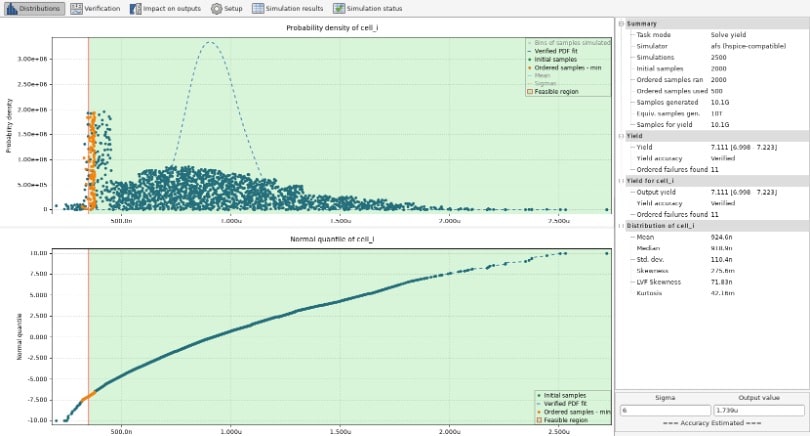
With this Solido AI approach, and the resulting Probability Density Function (PDF) would look like the example below:
Probability Density Function
Probability Density Function
The dashed blue line is the verified PDF fit. Green dots are the initial samples, and dark dots the Monte Carlo results. The orange dots are ordered samples.
For the actual bandgap reference circuit described in the presentation, Solido Variation Designer achieved verification equivalent to 10 billion brute-force simulations in just 24,100 simulations translating to a speed-up of some 415,000X.
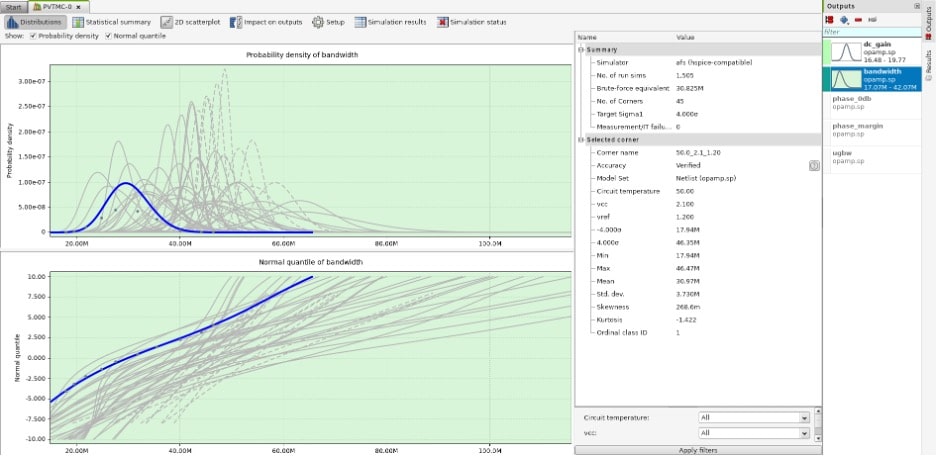
PVTMC Verifier covers all PVT corners and runs Monte Carlo in a way that requires only a few hundred simulations to capture the target sigma, thus reducing the number of simulations across the corners. The results are accurate as there are no extrapolations used or Gaussian assumptions, because it’s using real simulations at the target sigma. It’s covering all PVTs in a single run of the tool.
PVTMC Verifier example results
Inside of the PVTMC Verifier it’s identifying ordinals classes for all PVTs, capturing a distribution for each class, then verifying distributions within known classes. On the bandgap reference circuit described in the presentation, PVTMC Verifier ran a 6-sigma verification across all 36 PVTs in just 11,000 simulations, a speed-up of 32,000,000 compared to brute-force Monte Carlo.
The tool flow for using Solido AI is that a circuit netlist is run through PVTMC Verifier to select the worst-case statistical points, simulates the samples at multiple scales, observe the response to a change in scale, then it builds a model to predict the unscaled yield estimate. These first-pass results are then sent to the high-sigma verifier which runs initial samples until model building is successful, uses AI to generate Monte Carlo samples, then runs tail samples until the result is verified.
Using the Solido AI methodology required only 300 simulations per PVT with PVTMC Verifier (10,800 simulations) plus 20,000 simulations with High-Sigma Verifier, so a total of 34,900 simulations. The accuracy matched brute-force Monte Carlo, however the results completed 10,000,000X faster
Summary
At Samsung they are using Solido AI technology to achieve their goals of high-sigma verification across IC applications, while having much shorter run times than using brute-force Monte Carlo simulations. They used PVTMC Verifier to give first-pass results across all PVTs, then followed with High-Sigma Verifier for the final verification on critical and worst-case PVTs.
MOSFET gate resistance is a very important parameter, determining many characteristics of MOSFETs and CMOS circuits, such as:
• Switching speed
• RC delay
• Fmax – maximum frequency of oscillations
• Gate (thermal) noise
• Series resistance and quality factor in MOS capacitors and varactors
• Switching speed and uniformity in power FETs
• Many other device and circuit characteristics
Many academic and research papers have been written about gate resistance. However, for practical work of IC designers and layout engineers, many important things have not been discussed or explained, for example:
• Is gate resistance handled by SPICE models or by parasitic extraction tools?
• How do parasitic extraction tools handle gate resistance?
• How can one evaluate gate resistance from the layout or from extracted, post-layout netlist?
• How can one identify if gate resistance is limited by the “intrinsic” gate resistance (gate poly), or by gate metallization routing, and what are the most critical layers and polygons?
• Is gate distributed effect (factors of 1/3 and 1/12, for single- and double-contacted poly) captured in IC design flow (in PDK)?
• Is vertical gate resistance component captured in foundry PDKs?
• Should the gate be made wider or narrower, to reduce gate resistance?
• What’s the difference between handling gate resistance in PDKs for RF versus regular MOSFETs or p-cells?
The purpose of this article is to demystify these questions, and to provide some insights for IC design and layout engineers to better understand gate resistance in their designs.
Gate resistance definition and measurement
Gate resistance is an “effective” resistance from the driving point (gate port, or gate driver), to the MOSFET gate instance pin(s) – see Fig.1. (instance pin is a connection point between a terminal of SPICE model and resistive network a net).
Figure 1. MOSFET cross-section and schematic illustration of gate resistance.
However, the simplicity of the schematic in Figure 1 may be very misleading. Gate nets can be very large in size, contain many driving points, many (dozens of) layers (metal and via), millions of polygons, and up to millions of gate instance pins (connection points for device SPICE model gate terminals) – see Figure 2.
Figure 2. Schematic illustration of the top-view and cross-sectional view of MOSFET gate network
Gate network forms a large distributed system, with one or several driving points, and many destination points.
Very often, gate net looks and behaves as a huge, regular clock network, distributing the gate voltage to a FET.
Deriving an equivalent, effective gate resistance for such a large and complex system is not a simple and straightforward task. SPICE circuit simulation does not explicitly report gate resistance value.
Knowing the value of gate resistance is very useful to estimate the speed of switching, delay, noise, Fmax, and other characteristics, to see if characteristics are within the spec. Also, knowing the contributions to the gate resistance – by layer, and by layout polygons – is very useful to guide the layout optimization efforts.
Gate resistance handling by parasitic extraction tools
To understand gate resistance in IC design flow, it’s important to know how parasitic extraction tools treat and model it.
All industry-standard parasitic extraction tools handle gate resistance and its extraction similarly. In layout, the MOS gate structure is represented by a 2D mask traditionally called “poly” – even though the material can be formed by a complex gate metal stack and may have a complex 3D structure.
They fracture the poly line at the intersection with the active (diffusion) layer, breaking it into “gate poly” (poly over active) and “field poly” (poly outside active), as shown in Figure 3.
Figure 3. R and RC extraction around MOSFET gate.
Gate poly is also fractured at the center point. Gate instance pin of the MOSFET (SPICE model) is connected to the center point of the gate poly. Gate poly is described by two parasitic resistors, connecting the fracture points. A more accurate model of the gate poly, with two positive and one negative resistor, can be enabled in the PDK, but some foundries prefer not to use it (see next section on Gate Delta Model).
Parasitic resistors representing the field poly are connected to the gate contacts or to MEOL (Middle-End-Of-Line) layers and further to upper metal layers.
MOSFET extrinsic parasitic capacitance between gate poly and source / drain diffusion and contacts is calculated by parasitic extraction tools, and assigned to the nodes of the resistive networks. Different extraction tools do this differently – some tools connect these parasitic capacitances to the center point of the gate poly, while some other tools connect them to the end points of the gate poly resistors. The details of the parasitic capacitance connection to the gate resistor network may have a large, significant impact on transient and AC response, especially in advanced nodes (16nm and lower), where gate parasitic resistance is huge.
These details can be seen in the DSPF file, but are not usually discussed in the open literature or in foundry PDK documentation. Visual inspection of text DSPF files is tedious and requires some expertise. Specialized EDA tools (e.g ParagonX [3]) can be used to visualize RC networks connectivity for post-layout netlists (DSPF, SPEF), probe them (see and inspect R and C values), perform electrical analysis, and do other useful things.
Delta gate model
MOSFET gate forms a large distributed RC network along the gate width – shown in Figure 4.
This distributed network has a different AC and transient response than a simple lumped one-R and one-C circuit. It was shown [2-3] that such RC network behaves approximately the same as a network with one R and one C element, where C is the total capacitance, and R=1/3 * W/L *rsh for single-side connected poly, and R=1/12 * W/L * rsh for double-sided connected poly. These coefficients – 1/3 and 1/12 – effectively enable an accurate reduced order model for the gate, reducing a large number of R and C elements to two (or three) resistors and one capacitor.
To enable these coefficients in a standard RC netlist (SPICE netlist or DSPF), some smart folks invented a so-called Gate Delta Model – where a gate is described by two positive and one negative resistors – see Figure 5.
Figure 5. MOSFET Delta gate model.
Some SPICE simulators have problems handling negative resistors, that’s possibly why this model did not get a wide adoption. Some foundries and PDKs support delta gate model, while some others don’t.
Many people get surprised when they see negative resistors in DSPF files. If these resistors are next the gate instance pin – they are a part of the gate delta circuit.
Distributed effects along the gate length (in the direction from source to drain) are usually ignored at the circuit analysis level, due to a small value of gate length as compared to gate width.
Impact of interconnect parasitics on gate resistance
In “old” technologies, metal interconnects (metals and vias) had a very low resistance, and gate resistance was dominated by gate poly. The analysis and calculation of gate resistance was very simple.
In the latest technologies (e.g. 16nm and lower), interconnects have very high resistance, and can contribute a significant fraction (50% or more) to the gate resistance. Depending on the layout, gate resistance may have significant contributions from any layers – devices (gate poly, field poly), MEOL, or BEOL.
Figure 6 shows the results of gate resistance simulation using ParagonX [3]. Pareto chart with resistance contributions by layer helps identify the most important layers for gate resistance. Visualization of contributions by layout polygons to the gate resistance immediately points to the choke points, bottlenecks for gate resistance, that is very useful to guide layout optimization efforts.
Figure 6. Simulation results of gate resistance: (a) Gate resistance contribution by layer, and (b) contribution by polygons shown by color over the layout.
Gate resistance in FinFETs
In planar MOSFETs, the gate has a very simple planar structure, and the current flow in the gate is one-dimensional, along the direction of the gate width.
In FinFET technologies, the gate wraps around very tall silicon fins, and hence has a very complicated 3D structure. Further, gate material is selected based on the work function, to tune the threshold voltage (threshold voltage in FinFETs is tuned not by the channel doping, but by gate materials). These materials have very high resistance, much higher than solicited poly (which has typical sheet resistivity of ~10 Ohm/sq). The gate may be formed by multiple layers – interface layer with silicon, and one or more layers above it.
However, all these details are abstracted from the IC designers and layout engineers, and they see usual polygons for “poly” and for “active” – which makes design work much easier.
Handshake between SPICE model and parasitic extraction
In general, both SPICE models and parasitic extraction tools take gate resistance into account. Parasitic extraction is considered a more accurate method of calculating parasitic R and C values around the devices, since it “knows” (unlike SPICE) about the layout.
To avoid parasitic resistance and capacitance double-counting (in SPICE model and in parasitic extraction), there is a mechanism of a hand-shake between SPICE modeling and parasitic extraction, based on special instance parameters.
Regular device vs RF Pcell compact models
Regular MOSFET SPICE models do not describe gate resistance accurately enough for high frequencies, high switching speeds, or for RF or noise performance. To enable high simulation accuracy, the foundries usually recommend using RF P-cells, that have fixed size, that contain a shield (guard rings and metal cages), and that are described by high-accuracy models derived from measurements. However, these RF P-cells have a much larger area than standard MOSEFTs, and many designers prefer to use standard MOSFETs, to reduce area.
Vertical component of gate resistance
In “old” technologies (pre-16nm), gate resistance was dominated by lateral resistance. However, in advanced technologies, multiple interfaces between gate material layers lead to a large vertical gate resistance. This resistance is inversely proportional to the area of the gate poly. It can be modeled as an additional resistor connecting gate instance pin to the center point of the gate poly – see Figure 7(a). As a result, when the gate gets narrower (smaller number of fins), gate resistance goes down, but increases at very small gate widths. It displays a characteristic non-monotonic behavior, as seen in Figure 7(b). The old rule of thumb where “the narrower gate has lower gate resistance” does not work any more. Designers and layout engineers have to select the optimum (non-minimal) gate width (number of fins), to minimize gate resistance.
Figure 7. (a) Gate model accounting for vertical gate resistance, and (b) measured and simulated gate resistance versus number of fins (ref. [2]).Depending on technology, on PDK, and on foundry, the vertical gate resistance may or may not be included into parasitic extraction. It’s very easy to check this in DSPF file – if gate instance pin is connected directly to the center of the gate poly – vertical resistance is not accounted for. If it is connected by a positive resistor to the center of the gate poly – that resistors represents the vertical gate resistance.
Technology trends
With technology scaling, both gate resistances and interconnect resistances increase significantly – by up to one or two orders of magnitude. As a result, the details of the layout that were not important for gate resistance in older nodes, become very important in advanced nodes.
Other MOSFET gate-like structures
While the discussion on gate resistance in this article is focused on MOSFETs, the same arguments and approaches are applicable to other distributed systems controlled by the gate or by gate-like systems, such as:
• IGBTs (Insulated Gate Bipolar Transistors)
• Decoupling capacitors
• MOS capacitors
• Varactors
• Deep trench and other MIM-like integrated capacitors
Figure 8 shows a gate structure of a vertical MOSFET, and gate delay distribution over the device area, simulated using ParagonX [3].
Figure 8. (a) Typical layout of vertical FET, IGBT, and other gate-controlled devices. (b) Distribution of gate resistance and delay over area.
References
1. B. Razavi, et al., “Impact of distributed gate resistance on the performance of MOS devices,” IEEE Transactions on Circuits and Systems I: Fundamental Theory and Applications, vol. 41, pp. 750-754, 11 1994.
2. A.J.Sholten et al., “FinFET compact modelling for analogue and RF applications”, IEDM’2010, p.190.
3. ParagonX User Guide, Diakopto Inc., 2023.
Performance, Power and Area (PPA) metrics are the driving force in the semiconductor market and impact all electronic products that are developed. PPA tradeoff decisions are not engineering decisions, but rather business decisions made by product companies as they decide to enter target end markets. As such, the sooner a company knows if a certain PPA can be achieved, the better it is for business planning purposes alongside chip development work. The worst thing to happen is for a company to realize many months into the development phase that the desired PPA cannot be achieved. Hence, companies seek to establish optimal PPA for a chip as early as possible in the development process. Placement happens to be such a stage as the physical elements have more or less been finalized. But achieving that goal is not that simple given the several challenges related to PPA that need to be addressed to achieve a successful design.
What if there is a way to achieve optimal PPA at placement stage and carry it through to signoff, in spite of the above mentioned challenges. Siemens EDA’s digital implementation solution Aprisa promises to deliver that benefit and more. This was substantiated by MaxLinear, one of Siemens EDA’s customers during the recent User2User conference. Ravi Ranjan, MaxLinear’s Director of Physical Design presented proof points based from real life experience with N16 and N5 process based design implementations. MaxLinear plans to extend the adoption of Aprisa for new process nodes on future projects.
Excellent Correlation
One common reason for changing the placement after routing is to fix timing violations. The design needs to meet the required timing constraints while minimizing the delay and maximizing the clock frequency. This requires careful optimization of the placement and routing to ensure that the critical paths are optimized, and the timing constraints are met. Another reason for changing placement after routing is to optimize power consumption. The design needs to minimize the power consumption while still meeting the performance requirements. This requires careful power optimization techniques such as clock gating, power gating, and voltage scaling to minimize the power consumption. Yet another reason for changing placement after routing stage is to address routing congestion. Too many wires or interconnects that need to be routed through a limited space, result in routing difficulties or a suboptimal routing solution.
Closure is the process of meeting all design requirements, such as timing, power, and area, while also ensuring that the design is manufacturable.
Excellent correlation of timing, latency and skew through the placement, clock tree synthesis (CTS) and routing stages are indicative of placement stage PPA carrying through to successful routing. As an example, the following Figure shows pre-route vs post-route signal net length and clock net length correlation sample from a N16 based design.
Automated Flow Setups
Place and route (P&R) tools and methodologies typically need to be adapted for each new technology node to achieve the best PPA for a target process. The reason for this is that each process technology has unique characteristics that can significantly impact the P&R process. To achieve the best results, P&R tools need to be specifically calibrated and optimized for a process node. Typically, this step calls for engineering expertise and prior experience and involves trial-and-error for adoption.
Aprisa’s FlowGen capability reduces the effort needed to setup for new technology and adapt the design flow as well. MaxLinear found it very easy to adapt their flow when moving from N16 to N5 designs. The Aprisa FlowGen supports a wide range of design types including SoC, CPU, timing critical and congestion critical ones.
Summary of Aprisa Benefits
Placement stage optimal PPA maintained through to signoff
Anirudh is an engaging speaker with a passion for technology. Acknowledging the sign of the times, he sees significant value-add in AI but reminded us that it is a still supporting actor in system design and other applications where star roles will continue to be played by computational software that’s founded in hard science, math, and engineering technologies. This is Cadence’s singular focus—continuing to advance computational software methods in EDA and other domains while leveraging AI techniques where appropriate.
Market drivers
I was talking to an analyst recently who thought that because manufacturing activity is down, semiconductor design must also be suffering. So, I’m not surprised that Anirudh kicked off the discussion with a nod to this being a tough year for semi revenues following multiple years of massive growth, attributing the correction to over-stuffed inventories.
And yet (maybe someday analysts will understand this), design continues to be strong, in part because design cycles are much longer than manufacturing cycles, in part because no one can afford to come out of a downturn without new products ready to launch, and in part because design starts continue to grow as systems companies, now delivering 45% of Cadence business, are accelerating their own design activity.
Anirudh believes that the semi-industry will reach $1 trillion in revenue by the end of the decade, a 2X growth from today, and that electronics and related systems will reach $3 trillion in revenue in a similar period. Manufacturing may be in a slump right now, but we already have an appetite for hyperscale computing, 5G, autonomous vehicles, AI and industrial IoT. That appetite won’t disappear, so manufacturing will surge back at some point. The winners at that point will be companies ready with new designs. Cadence is very optimistic about the long-term tailwinds behind design for such products.
Computational software and AI
Computational software is all about precision at a massive scale of complexity of the object to analyze (billions to soon trillions of transistors) and in the nature of the analysis (PPA optimization and/or multi-physics). Foundational methods are grounded in well-established hard science advances like finite element analysis with origins in the late 1800’s. Maxwell’s electromagnetic equations from a similar period, thermal diffusion first described by Fourier even earlier, and so on and so on. The EDA industry has been developing technologies over at least the last 50 years.
In contrast, AI is all about probabilistic inferencing, delivering impressive responses with, say, 97% certainty, in some cases better than we can manage. But, at the same time, we don’t want to hear that in 97% of cases our car won’t crash, or the robot surgeon won’t make a mistake. We want the precision and reliability of computational software in building and analyzing systems with AI as a layer on top to help us explore more implementation options.
Developing and maintaining that technology is not cheap. Cadence has about 10,000 people with 65% in R&D and 25% in customer support. 90% of its staff are in engineering, which is comforting to know. Designs built using these technologies will be reliable, safe, secure, and eco-friendly. But how does that scale? By 2030, designs are expected to grow by at least 10X in transistor count. Technology companies are already struggling to add staff, but none can afford to grow staffing by 10X. We need to become even more efficient by abstracting architecture design to higher levels, parallelizing even more, and relying more on AI-assisted decision-making.
AI in Cadence products
Reinforcement learning has become a dominant technique for optimization in EDA. One significant advantage is that it doesn’t require gradient-based estimation to find good search directions to advance. Gradient methods work well when optimization metrics vary relatively smoothly and can be computed quickly but not if they vary rapidly or take hours to compute on each change. Cadence has been talking over the past couple of years about advances in AI with the delivery of products like Cadence Cerebrus, Verisium and Optimality, which all utilize reinforcement learning over multiple runs to guide optimization. These are all cases where computing metrics with precision may take hours, making reinforcement learning essential to advance optimization options.
Evidently results are impressive, as judged by numbers Anirudh shared. There have already been 180+ Cadence Cerebrus tapeouts.
Last month, Cadence announced Virtuoso Studio, covered in more detail by my colleague Daniel Payne. Briefly, this offers more place-and-route support in analog and a claimed 3X productivity advance for designers. There’s more support for heterogenous integration in 2.5D/3D packaging, adding analog and RF into the same package. It also includes integrations with the digital design tool suite, integrity analysis, multi-die packaging, AWR analysis and multi-physics analysis for thermal, electromagnetics, etc.
Cadence also recently announced Allegro X AI for PCB and package design, which it automates placement and routing and reduces physical layout and analysis challenges. For 3D-IC Cadence offers Integrity, starting development in Allegro back in 1995, long before most of us had even heard of chiplets (remember system in package and modules?). Around 2015, more capabilities were developed, though the industry was still not quite ready. More recently, Cadence has been working very closely with its foundry partners to refine Integrity support leading to their latest AI-driven 3D-IC solution.
Onward and upward
It’s easy to see the computational software focus in everything I described above—from chip design and analysis to package and system design and analysis. Where is Cadence going with some of their recent acquisitions? In May of last year, Cadence announced a partnership with the McLaren Formula 1 team who are looking to its Fidelity CFD software to optimize aerodynamics for McLaren’s race cars.
Cadence acquired Future Facilities about a year ago. They provide electronics cooling analysis and energy performance optimization solutions for data center design and operations using physics-based 3D digital twins. Just to prove they are even more versatile, only a few days ago, Cadence announced a partnership with the 49ers, to evaluate ways to optimize energy efficiency and sustainability at Levi’s stadium.
Last year, Cadence also made an investment in molecular sciences company, OpenEye Scientific. Anirudh is very excited about this, seeing huge synergy in simulating molecules. He sees (of course) significant similarities between OpenEye simulation and the Cadence Spectre platform with physics models for molecules looking rather like BSIM models for circuit simulation!
Energizing stuff. I look forward to next year’s update.
The flexibility of RISC-V processor IP allows much freedom to meet specific requirements – but it also opens the potential for many bugs created during the design process. Advanced processor features are especially prone to errors, increasing the difficulty and time needed for thorough verification. Born out of necessity, Codasip has pioneered a formal-based RISC-V processor verification process, bringing higher-level simulation and formal verification methods to efficiently verify core modifications, as shared in their latest technical paper.
Digital logic simulation in complexity only scratches the surface
Simulation seems like an ideal solution for digital logic, and it does shake out many bugs in a first pass that runs quickly. It’s logical to think that by simulating functional blocks individually, combining them into a complete design, and simulating it again, coverage would be pretty good.
As it turns out, pretty good is not nearly good enough. Simulation is only as good as the models and conditions applied – and in a complex RISC-V setting, uncertainty prevails. What software is running, which asynchronous events occur, and how the processor transitions from state to state in every possible scenario can be extremely time-consuming to model for simulation. If a simulator stumbles on a problematic corner case, it may only be sheer luck.
L31 block diagram. Source: Codasip
A good example is a branch predictor, such as the block shown in the Codasip L31 RISC-V processor IP. A myriad of states need to be set up to simulate completely how the branch predictor behaves in all cases of caching and pipeline execution.
Codasip uses the word “impossible,” but covering all state space in simulation is impractical, given finite engineering resources and time limits. They see simulation as an essential but not a standalone tool in the formal-based RISC-V processor verification process.
Combining techniques for better coverage in less time
Codasip outlines several advantages of applying formal verification as a complement to simulation.
Design behaviors are specified using assertions. Assertions are used both in simulation and in formal. In formal, however, a mathematical analysis can sometimes uncover corner cases that the random walk of simulation has a low probability of hitting.
Formal can also tackle non-functional verification such as clock-gating, X-propagation, and clock domain crossing.
Formal verification handles investigations where debugging information is limited, providing a way to classify and identify bugs for detailed analysis.
Manually writing assertions remains a problem, especially if one has to go back to write all the assertions for a complex design from scratch. The nice thing about RISC-V being an open architecture is many people are looking at the challenges, including verification. If a team could build on existing assertions from the RISC-V community and incrementally define new ones for their adjustments and additions, it would speed up formal verification.
Codasip has gone one step further, grabbing a golden RISC-V instance. The Siemens OneSpin Processor Verification App consists of a single-cycle execution model of the RISC-V ISA and a set of template assertions to check a design against this model. Codasip has instantiated this model together with the design and specialized the assertions to “connect” both, taking care of the pipeline and other specificities.
End-to-end verification flow for the 3-stage L31 core (when the verified instruction I is neither stalled nor flushed). Source: Codasip.
Automatically is the operative word. In this approach, users can specify RISC-V parameters and extensions, extract design data, add customizations like new instructions, and move to verification without spending time writing assertions manually or trying to split the design into smaller chunks. Codasip has demonstrated verification of the full L31 at once in this approach.
Cutting formal-based RISC-V processor verification down to two hours
The punchline of this technical paper is Codasip reduced the time to verify the L31 core from thousands of simulation hours – assuming that a simulation scenario could even be generated, what could be person-years of effort – to full proof in two hours of run time after setup.
And they didn’t skip steps. They outline three complex corner cases where the approach spotted bugs they didn’t anticipate from the simulation. A branch predictor corruption arose when an undefined instruction generated an exception. Delays and pipeline stalls in the right combination caused multiple executions of the same instruction. A legal FENCE.I instruction got incorrectly marked as illegal.
Codasip uncovered 15 bugs in the formal-based RISC-V processor verification effort for the L31 that their simulations and other steps missed. Design quality increased, and the process laid the path to faster verification of future customizations for their customers.
To get the whole story, download the Codasip technical paper (registration access for full text):
Dan discusses the recent Q4 2022 ESDA report with Wally Rhines, Executive Sponsor of the SEMI Electronic Design Market Data report. Overall, the report portrays strong growth and positive results. Dan explores some anomalies in the data and possible reasons with Wally.
Dan also discusses some very interesting events at the upcoming Design Automation Conference with Wally. You won’t want to miss those.
The views, thoughts, and opinions expressed in these podcasts belong solely to the speaker, and not to the speaker’s employer, organization, committee or any other group or individual.
A Petri nets blog scored highest in engagement last year. This month we review application of the technique to validating an expanding range of JEDEC memory standards. Paul Cunningham (Senior VP/GM, Verification at Cadence), Raúl Camposano (Silicon Catalyst, entrepreneur, former Synopsys CTO and now Silvaco CTO) and I continue our series on research ideas. As always, feedback welcome.
JEDEC standards for memory protocols describe the complexities of command behaviors and timing through a mix of state machine diagrams, tables, and timing diagrams. Validating an implementation through simulation depends on creating meaningful tests and checks through manual comparison with the standard doc. JEDEC themselves acknowledge that their reference based on a combination of FSMs, tables and timing diagrams is not fully complete and makes automated test generation problematic. This paper uses Timed Petri Nets to provide a full model of the DRAM states, the logical command dependencies and the internal timing dependencies of the system under test, from which a complete SystemC reference model can be automatically generated and used as a reference with popular DRAM simulators for verification.
In addition to the value of the ideas, this paper provides a useful intro to the mechanics of DRAM operation for novices like me!
Paul’s view
This is an easy to read, self-contained paper, providing a great example of the opportunity for domain specific languages in design and verification. In this paper the authors tackle the problem of verifying DDR interfaces. They build on prior art describing the DDR3 protocol using a Petri Net, a wonderful graph-based notation for visually representing interactions between concurrent state machines.
The authors’ key contribution is to upgrade this prior art to a “Timed” Petri Net containing additional arcs and annotations to model the timing dependences between commands in the DDR protocol standard. They create a nice little textual language, DRAMml, for describing these Timed Petri Nets which is able to represent the complete DDR3 command protocol on one page. Nice!
They also develop a compiler for DRAMml to generate simulatable SystemC code which can be used as a “golden” model as a reference for verification. As final icing on the cake, they use their golden model to find a bug in DRAMSys, a well cited popular DRAM simulator in the literature. I would be really interested to see if this work could be applied to other protocols such as PCIe or Ethernet.
Raúl’s view
This is the first paper on the validation of dynamic memory controllers for DDR that we have reviewed in this series. JEDEC has issued 19 standards since the original DDR in 2000, including DDR5 and HBM3. It is easy to see that the specification of such memories – with multiple banks, 212 to 218 rows, where each row can store 512 B to 2 KB of data, recharge, refresh requirements – can get very complex, particularly regarding the timing requirements. As an example, the authors cite that to model the complete state space of a DDR4 with 16 banks requires 65,536 states with over a billion transitions.
To simplify and formalize memory specifications, the paper builds models using extended Petri Nets. Petri nets are bipartite graphs with places and transitions connected by weighted directed arcs (section 3.2). They are extended by:
-> [t1, t2] timed-arc with guard [t1,t2] meaning the transition can only fire in that time interval
->> reset-arc which clears a place of all tokens
-o inhibitor-arc which prevents a transition to fire
With such extensions Petri Nets become as powerful as Turing Machines. These Petri Nets model DRAMs with reasonable complexity, e.g. 4 places and 8 transitions, plus a place and 6 transitions per bank. Power can be modeled directly; timing gets a bit more complicated requiring also timing dependencies between transitions.
The paper then goes on to define a DSL (domain specific language) called DRAMml using the MPS Software from Jetbrains, to describe this Petri Net and convert it to SystemC. The generated executable model was simulated with several DRAM simulators, namely DRAMSim2, DRAMSys, Ramulator, and the DRAM controller in gem5, uncovering a timing violation in DRAMSys.
I found the paper interesting and easy to read given that I also worked with Petri Nets before. Following the DRAM specs in detail is more for the specialist but can be educational. The claim that “DRAMml, which describes all the timing, state and command information of the JEDEC standards in a formal, short, comprehensive, readable and understandable format” is not obvious. It requires understanding of Petri Nets, which may be a barrier to the adoption of the methodology, despite improved simplicity and expressive power. It would be interesting to know what JEDEC thinks of this approach since in principle it should allow them to provide or at least build definite reference models for new standard releases.
Dan is joined by Nigel Drego, the CTO and Co-founder at Quadric. Nigel brings extensive experience in software and hardware design to his role at Quadric. Nigel is an expert in computer architectures, compiler technology, and software frameworks.
Dan explores the unique and unified HW/SW architecture developed by Quadric with Nigel. The benefits of a single architecture programmable approach to on-chip AI is explained, along with specific examples of how to adapt the system to various AI processing challenges.
The views, thoughts, and opinions expressed in these podcasts belong solely to the speaker, and not to the speaker’s employer, organization, committee or any other group or individual.


