
Arm recently announced an update for mobile under the Arm Total Compute Solutions (TCS) label, led by Chris Bergey (Sr. VP/GM for the Client line of business). You’ll remember that Chris headed the infrastructure line of business impressively through the Neoverse brand, as demonstrated by Arm-based servers appearing in multiple hyperscalars and penetration in multiple wireless infrastructure platforms. Now we get to see what he can do with mobile.
How do you grow in a saturated market?
That’s the challenge for Arm. The engine that boosted them to fame and fortune, the smartphone business, now sees declining unit shipments and projections for revenue growth anywhere between 2.5% and 7% CAGR depending on who you believe. The spread reflecting, I’m sure, uncertainty in what might stick among future product features.
Arm sees mobile gaming as an important TAM growth driver, consistent with their view last year. They commissioned a report a couple of years ago showing that mobile gaming is by far the most popular platform for gaming worldwide. Given that gaming is even now a significant contributor to NVIDIA revenue, I can believe mobile gaming presents an opportunity for Arm.
Arguably today the mobile gaming trend is strongest in China where consumers are very active in online multi-player games. Chris sees folding phones accelerating the trend as these offer a larger screen size. I also remember that at least last year the majority of phones in China were still on 3G. I expect need to upgrade to 4G/5G would also push growth, especially for Chinese phone suppliers (Xioami, Oppo, Vivo, etc). RISC-V could in theory compete for CPU slots, but without a top-of-the-line GPU offering and NVIDIA blocking RISC-V support for their GPUs that threat seems limited for now.
Gaming is also popular outside China mostly in puzzle-oriented games rather than hard-core player-competition titles. Arm sees this changing already in Korea and expects growth in the West as content adapts and as larger screen options (especially foldables) become more popular. Seems reasonable – we’re already starting to see Galaxy-S23 commercials in the US for competitive gaming; the seed is being planted 😊. Arm’s point here is that mobile competitive gaming demands a high level of performance in a smartphone, in CPUs and GPUs, features that will only be possible in premium models.
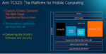
What’s new in TCS23?
There are 4 new cores covered under the announcement. Given the gaming focus of this release, Chris led with the new Immortalis G720 GPU, developed in partnership with MediaTek. Arm have upgraded the graphics pipeline to support the more complex real-time 3D imaging already standard on console and PC applications. This comes with a 15% uplift in performance and efficiency and a boost in system-level efficiency. They also introduced Mali-G720 and Mali-G620, presumably targeted to entry-level gaming handsets.
Next up is the Armv9 Cortex CPU compute cluster, starting with the Cortex-X4, delivering 15% more performance than Cortex-X3 at 40% less power and expected to serve AI/ML applications. There are new big and LITTLE cores – Cortex-A720 for “big” and Cortex-A520 for “LITTLE”, both delivering 20% power efficiency improvements over earlier generations. There is also a DSU update. Chris notes that there is now a tighter coupling between process nodes and these performance metrics, enabled by close collaboration with TSMC. That may account for these cores being 20% more area efficient than the nearest competitor, per Chris.
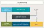
All of these cores are now 64-bit and complemented by Arm Memory Tagging Extension (MTE) to eliminate memory safety bugs. 70% of security issues detected in Microsoft products and 75% of vulnerabilities detected by Google in Android have been attributed to memory safety problems, leading Google to adopt MTE for Android. Nice – I’m impressed by the work Arm is putting into security, here and in the Cheri collaboration.
Deployment
The platform is built into the MediaTek Dimensity 9200, which in turn is inside top of the line phones from Oppo and Vivo and is already delivering results in games from Genshin Impact to Fortnite. Chris didn’t want to share more details but seems optimistic that more deployments will be announced.
In summary, growing in a saturated market will be an uphill climb, but Arm seems to know how it wants to get there and continues to work on ensuring it will stay on top of the game through continued technology advances. You can read the press release HERE.


