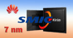
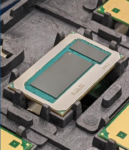
Banner 800x100 0810

Podcast EP115: Virtualize Your Development of Arm-Based Designs and More with Corellium

Podcast EP115: Virtualize Your Development of Arm-Based Designs and More with Corellium
by Daniel Nenni on 10-21-2022 at 8:00 am

Dan is joined by Bill Neifert, Senior Vice President of Partnerships at Corellium. Prior to Corellium, Bill was Senior Director of Marketing for Arm’s Development Solutions Group. Before that he was the co-founder and CTO of Carbon Design Systems which was acquired by Arm.

Dan explores the virtualization technology of Correlium with Bill. How their products help with Arm-based design development and some of the plans to extend the technology beyond Arm designs.

The views, thoughts, and opinions expressed in these podcasts belong solely to the speaker, and not to the speaker’s employer, organization, committee or any other group or individual.


CEO Interview: Aleksandr Timofeev of POLYN Technology

CEO Interview: Aleksandr Timofeev of POLYN Technology
by Daniel Nenni on 10-21-2022 at 6:00 am

2022 AT foto 3

Aleksandr Timofeev is CEO and Founder of POLYN Technology, an innovative provider of ultra-low-power high-performance NASP (Neuromorphic Analog Signal Processing) technology. Alexander is a serial entrepreneur with more than 20 years in the high-tech industry. Prior POLYN, he founded iGlass Technology, a company that developed novel electrochromic smart glass technology. He built the core team, general technology, and product concept and successfully sold the company at the end of 2020 to a strategic investor. Aleksandr is also founder and managing partner at FPI VC team, an early-stage venture investment management company. The fund focuses on early-stage innovative companies, developing clear product concepts and strategies and working with venture firms and partners for subsequent funding rounds.

While looking at the landscape of new startups in the AI/ML industry I found POLYN. The company differs from others in its business model as well as its concept and technology approach.

POLYN is a fabless semiconductor company selling ready-to-use Analog Neuromorphic chips as Application Specific Standard Products, targeting specific technological challenges in huge and fast-growing markets, particularly wearables, connected health, and Industry 4.0. Founded in 2019, it is registered in the UK with HQ in Israel.

According to its website, POLYN offers two products, and one more is under development. Recently it was announced that POLYN was accepted into the Silicon Catalyst incubator family.

We talked with Aleksandr Timofeev, CEO and founder, to explain the technology and what he is up to now. We asked Aleksandr’s opinion on today’s neuromorphic computing, what is special about POLYN, and how far we are from a real Tiny AI solution working on the sensor level. Here’s the interview:

Q: First, congratulations on joining the Silicon Catalyst incubator Could you say few words about what is in it for POLYN?

AT: POLYN’s objective as a fabless semiconductor company focusing on ready-to-use analog neuromorphic chips is to collaborate with leading semiconductor vendors, industry partners, and entrepreneurs.  Our mission is to introduce novel analog neuromorphic solutions for wearables, hearables, and IIoT on-sensor pre-processing with highly efficient energy per inference ratio. By being part of the Silicon Catalyst community and its huge portfolio of partners, we expect to accelerate our plans to improve cost, time to market, and the reach of our unique technology.

Q: I see your company decided to go a different way with constructing a chip from a neural network, unlike many others who are developing general purpose processors to apply a neural network there?

AT: Yes, we decided that for a neuromorphic based product it is more efficient to synthesize a chip from a neural network model, not like in the digital domain where you have fixed, general purpose PU instruction sets, and different software applications using them. When you start training a neural network (NN), you don’t know what final size you will get. If you have a fixed neuromorphic core, for some NNs it will be too small, and for others too big.

Q: Ok, interesting, but that means you need to generate a lot of chipsets and that would be both time and cost consuming. How you are dealing with that challenge?

AT: We are focused on the ASSP model. Our chip is related to sensor or signal type, but not a sensor model. For example, our Voice Extraction NASP chip works with any type of analog or digital mems microphone and other signal sources. And we will generate a new NASP core only for a new sensor or signal type. As you understand, it covers millions of products.  In case some new product moves to a different physical device, we can upgrade the chip easily, thanks to our fully automated process. So, to summarize, first NASP is application-specific and not product-specific, so the volumes are huge. Second, moving from application to application is easy with the POLYN automation tools. By the way, our tools were the first technological achievement at the beginning of the company, and they remain a unique EDA instrument for neural network conversion.

Q: Very impressive, but I have another question: Your critics could say that implementing even the inference neural network models requires changes, and as a result your neural network will need tuning from time to time. If your technology is implemented in a fixed resistor layer, how do you support neural network changes and updates?

AT:  First, we use the fundamental property of a neural network: when you train a deep neural network, after a few hundred training cycles a major part of the layers will become frozen.  So typically, about 90% of layers are not changing anymore, and are not involved in the following updates. Only a few last layers require an update if you need to change the classification. In such case we use a hybrid solution:  the 90% layers are converted into a high performance NASP core and the last 10% remain in the flexible digital domain.  But it is important to remember that our solution is focused on sensor level applications. We are not simulating brain functions, where constant learning (or re-training) is critical. In many sensor-level applications the pre-processing task is fixed and doesn’t require any update.

Q: Let’s discuss the analog part. I mean, who would imagine we come back to analog after getting digital with millions of transistors on a chip and talking today about 2nm process? Why do you think analog is a right option for complex math models as neural networks?

AT: First of all, we talking about neuromorphic analog, which is not like old style analog computers. We represent a trained neural network using analog neurons. The fundamental property of this structure is true parallel data processing.

Any digital system has step-by-step execution. But the human brain, one of the most power-efficient computation devices, uses parallel data processing. It is important to note that POLYN is mimicking not the central brain but peripheral systems. We are at the sensor level where the main idea is pre-processing, removing noise, extracting data, and here the analog is irreplaceable. Digital can go down in the process, but for Joule per Inference ratio, analog will win.

Q: Any more arguments for analog? F

AT: First of all, we are talking about neuromorphic analog, that represents a trained neural network using analog neurons. The fundamental property of this structure is true parallel data processing.

Any digital system has step-by-step execution. But the human brain, one of the most power-efficient computation devices, uses parallel data processing. It is important to note that POLYN is mimicking not the central brain but peripheral systems. We are at the sensor level where the main idea is pre-processing, removing noise, extracting data, and here the analog is irreplaceable. Digital can go down in the process, but for Joule per Inference ratio, analog will always win.

Q: Any more arguments for analog? For example, how do you resolve the analog implementation noise issue? What is the product deviation on the math model?

AT: The answer again lies in the term “neuromorphic,” as neural networks are implemented in a neuromorphic analog circuit. The point is that resilience to errors is a fundamental property of neural networks, and training increases the resilience.

Circuit non-idealities can be divided into two groups: random and systematic errors.

Systematic errors occur because a typical circuit implementation only approximates an ideal signal processing operation to a limited extent. Such errors are caused, for instance, by the non-linear operating characteristics of devices or by finite gain of an analog amplifier.

Stochastic errors may happen during the fabrication of integrated circuits and result in a random variation of the properties of the fabricated on-chip elements. These errors, however, can be modelled and addressed during development. For example, the mismatch between neighboring elements is usually much smaller than the variation of parameters’ absolute values. Therefore, differential architectures could significantly improve precision.

For an analog circuit design, it is important that such errors do not accumulate. For this, the neural networks are trained using special technology for error compensation

Q:  Interesting. Could tell us about the birth of POLYN and the idea of your technology?

AT: I met Dmitry Godovsky, our Chief Scientist, at the end of 2018. Dmitry worked eight years previously on a new math model of converting a digital neural net to a new implementation. After few months of discussion, we understood that this new model can be represented as a neuromorphic analog circuit. So, in April 2019 we launched POLYN Technology. Since then, we have constantly invested in know-how and innovation. Today we have 25 patents for the technology and products.

Q: Naturally, this raises the question: what about FABs? Could they run the fabrication immediately, or they need to adapt their processes? By the way, the same question applies for the PDK and EDA tools you are using for the chip development.

AT: Our strong advantage is that we are using any standard process in 40-65 nm range and can align our product libraries to any standard PDK. Our NASP compiler and physical design module work on top of existing standard EDA-based design flow. The output is a GDSII file ready for tape out immediately. Together with that we have developed our design as a BEOL, so the resistor layer is mask programmable and could be replaced independently to optimize cost and time to market. The EDA tool, we call it T-Compiler, is important for time to market today and for our business model in the future. Right now, we are selling chipsets and IP Blocks. By the way, we also see that the market of chiplet solutions could be covered, since SiPs (systems in package) are becoming increasingly these days.
But once the technology is proven and more customers see the advantage of NASP for medium and higher volume products, then our T-Compiler tool will be a part of our business model, enabling generation of application-specific Neuromorphic Analog chips for specific tasks.

Q: Great clarification, thanks. Let’s now talk in general about when you think it makes sense to convert a neural network into silicon. What applications are you covering by the NASP solutions?

AT: We focus on any type of one-dimensional signal preprocessing, such as voice, health care sensors, accelerometer, or vibration sensors. And some of our solutions you can evaluate already with simulation that enables evaluation of the chip before its synthesis, to reduce the chance of unexpected behavior. Anyone who is looking for always-on smart sensor data pre-processing is more than welcome to contact us and get access to our D-MVP simulation model. For example, voice extraction and voice detection for hearing assistance demos are functions and running already. So, customer can evaluate and start the design in advance to be ready when the first chip will come from the factory by Q2 of 2023. Customers can also influence the functionality if they are in time to catch the last changes, we are doing these days.

Q: And what is your product strategy?

AT: Three directions are in our scope of activities for 2023, wearables, hearables, and vibration monitoring for predictive machine maintenance. The first product is planned for mid-2023 and it is our voice extraction solution we announced a week ago. The name of the product line is NeuroVoice and it is intelligent voice extraction and processing for the next generation of smartphones, earbuds, hearing aids, microphones, smart speakers, and intercoms. POLYN’s NeuroVoice NASP chip solves the problem of communication in a noisy environment. This differs from noise cancellation and can answer such challenges as irregular noises like animal sounds, babies crying, and sirens. It also solves the problem if  the sound comes over the network already mixed with noise. Together with voice extraction, NeuroVoice offers a combination of voice management features such as voice activity detection, keyword spotting, and others. In addition, the product can be customized for special requirements.

Q: Was it easy to raise money? I know that the situation changes every time.

AT:  Raising money is never easy (smiling). Of course, we worked hard to communicate with investors. We have a few VCs joining us and several more currently in the due diligence process. That is where we anticipate value in joining the Silicon Catalyst incubator, with the increased exposure we will gain through the incubator’s huge portfolio of partners.

Q: What do you think about neuromorphic chips today? Those like Intel Loihi, BrainChip and others around?

AT: We can discuss other solutions and compare performances, but in general, I can say that in our opinion they are targeted to a more centric position on the edge, with power consumption of a hundred milliwatts to a few watts, but POLYN is focused on the micro-watt level of the thin edge.

Q: And the final question. As a visionary, how do you see the neural-network- on-chip market and ways of its development? Would it be digital, in-memory, or similar to NASP?

AT: For some time, I think, things will run in parallel, and each technology will try to find niches, but finally, in my opinion, the future lies in self-organizing structures, like NASP, but with different physical principles of neurons.

Q: On that note, thank you very much, Aleksandr.

AT: Thanks a lot for the opportunity, and let’s meet in mid-2023 when the first NeuroVoice chip will roll off the line.

Also Read:

CEO Interview: Coby Hanoch of Weebit Nano

CEO Interview: Jan Peter Berns from Hyperstone

CEO Interview: Jay Dawani of Lemurian Labs


Clock Aging Issues at Sub-10nm Nodes

Clock Aging Issues at Sub-10nm Nodes
by Daniel Payne on 10-20-2022 at 10:00 am

IC failure rate chart, clock aging

Semiconductor chips are all tested prior to shipment in order to weed out early failures, however there are some more subtle reliability effects that only appear in the longer term, like clock aging. There’s even a classic chart that shows the “bathtub curve” of failure rates over time:

IC failure rate chart

If reality and expectations don’t align in the wear out region, then the financial impact of recalling chips embedded inside of systems can cost millions of dollars or even cost human life in safety critical applications.

A 7nm SoC can have 10 billion transistors, and to meet the power spec there are many clock domains, and multi-voltage power domains; resulting in aging issues like jitter, duty cycle distortion, insertion delay, reduced design margins, and increased process variation. To predict the impact of transistor aging requires knowing the circuit topology, switching activity, voltages and even temperature – a complex goal.

Transistor aging comes about from a few effects: Hot Carrier Injection (HCI), Negative Base Temperature Instability (NBTI), Positive Base Temperature Instability (PBTI). Hotter temperatures accelerate these effects. The duty cycle impacts BTI effects, and frequency has a proportionate effect on HCI. With HCI there are charges that get trapped in the oxide layer of the transistor, changing the Vt of the devices permanently. The BTI effect is higher than the HCI effect for 7nm nodes, as shown in this chart of insertion delay, where the black line is a fresh circuit, while aging effects from HCI are orange, and BTI effects are in blue.

BTI and HCI Effects

IC design methodologies above 10nm used Static Timing Analysis (STA) and some SPICE simulations of the clock, along with guard-banding for parameters like jitter. Aging could be applied across all devices to provide an idea of the electrical and timing impacts.

Under 10nm designs require a more comprehensive analysis of clock aging impacts, and Infinisim has created a tool called ClockEdge that analyzes large clock networks efficiently. The ClockEdge tool automatically creates a transistor-level netlist for analysis, and then can simulate overnight to show you the fresh and aged results.

A new clock domain netlist is created from your existing files: Verilog, Lib, leaf cell definitions, constraints, SPEF. Simulation results are generated with full SPICE accuracy at your functional clock frequency for the fresh state. The clocks are then stressed as the second step of analysis. A third step is to use the aged clock domain netlist, run the full SPICE accurate simulation at the functional clock frequency and evaluate duty cycle distortion, insertion delay, rail to rail levels, and even clock slew rates. The difference between fresh and aged results tells the design team if they have a reliable design or not.

Delving into the first step, the fresh run analyzes the clock domain from the output of a PLL, all the way through to flip-flops or output pads. This clock domain can be quite large in size with millions of devices, and the transistor-level analysis results show us the delay and slew values.

Step 1: Fresh Run

The ClockEdge tool can run clock analysis for a fresh run on a block with 4.5 million gates, 517 million MOSFETs and 3.2 billion devices overnight, by using a distributed SPICE simulation approach. Your clock topology can be implemented as trees, grids and spines.

Step 2 is a stress run where specific transistors will be selected for aging, all depending on the circuit topology and if the clock is being parked (stuck at VDD or  VSS), or toggling. The stress run also depends upon temperature, voltage and duration per usage model.

The final analysis is Step 3, using the Aged devices. For the case of devices that had a parked clock value, then only one edge of clock will be affected during aging analysis, while devices with clock toggling will have both edges affected during aging analysis. So the Duty Cycle Delay (DCD) shape will depend on your circuit topology.

Step 3, Aged Simulation

With ClockEdge a designer can perform what-if stress analysis, comparing the impact of a clock parked at 0, parked at 1, toggling, or even a combination of parked and toggling.

Summary

Clock aging is a new reliability concern, especially for IC designs at sub-10nm process nodes. With proper analysis, the effects of aging can be mitigated. Infinisim has the experience in analyzing the effects of clock aging. The ClockEdge tool from Infinisim is focused on giving designers accurate aging analysis of their clock networks, providing results quickly overnight. You get to see both DC and AC stress conditions for your aged clock domains.

Related Blogs


NIST Standardizes PQShield Algorithms for International Post-Quantum Cryptography

NIST Standardizes PQShield Algorithms for International Post-Quantum Cryptography
by Kalar Rajendiran on 10-20-2022 at 6:00 am

Signature Schemes Standardization Process

News of cyberattacks is routine these days in spite of the security mechanisms built into widely used electronics systems. It is not surprising that entities involved with ensuring safe and secure systems are continually working on enhancing encryption/decryptions mechanisms. Recently NIST standardized cryptography algorithms for the post-quantum computing world. PQShield is a company that is at the forefront of post-quantum cryptography and developing solutions to protect systems against quantum cyberattacks. The company announced that NIST has adopted an algorithm PQShield developed as one of several new post-quantum cryptography standards. An additional PQShield developed algorithm is moving to Round 4 of the NIST post-quantum cryptography standardization project.

To understand the significance of NIST’s standardization and PQShield’s announcement, it is important to get an overview of why new standards are needed, what the standardization process entails and how to deploy the new standards in one’s systems. PQShield has published three technical whitepapers that together cover the subject matter in detail. If you are involved in developing chips and software to deliver cybersecurity solutions, these whitepapers would be very informative. Links to download these whitepapers can be found in relevant sections of this blog.

The Threat from Quantum Computers

A quantum computer can perform computations much more efficiently than classical computers that have been common place to date. Maybe twenty years ago, quantum computing appeared far away, but we are now much closer to seeing quantum computers in commercial deployment. While this is great from a computing perspective, quantum computing capabilities can also easily break current security mechanisms.

RSA and ECC cryptosystems that are currently in use for secure data transmissions are easy for quantum computers to solve using Shor’s algorithm. This will open up systems for forgery of digital signatures (Integrity compromise) and decryption of previously encrypted data (Confidentiality compromise) in the future. This latter threat is considered the “Harvest Now, Decrypt Later (HNDL)” attack. Without being discovered, would-be attackers are regularly collecting and storing encrypted data with the expectation of deciphering the stolen data using quantum computers.

Based on history, we know it takes a long time to upgrade to new security standards. For example, the migration from Data Encryption Standard (DES) to Advanced Encryption Standard (AES) has taken decades. To be specific, the National Institute of Standards and Technology (NIST) established the AES standard in 2001. As such, newer security standards have to be established now, to protect against cyber threats from quantum computers.

Post-Quantum Cryptography (PQC)

The best way to mitigate the threat of attacks using quantum computers is to use quantum-safe cryptography. This post-quantum cryptography is being mandated by governments across the world for adoption by businesses who want to do business with these governments. With a likely deadline for adoption within the next three years, businesses will be forced to implement quantum-safe mechanisms quickly. But without a standard for international adoption, interoperability will become a practical roadblock.

For a detailed overview of Post-Quantum Cryptography, download this whitepaper.

The NIST Standardization Process

While a number of standardization efforts are currently underway (in Europe, China, etc.,), the NIST standardization project is the most well documented. The project was announced in 2016 with the goal of standardizing post-quantum signature schemes and key-establishment schemes.

In July 2022, NIST announced that it has selected the following three signature schemes as standards for PQC.

Primary standard:           Dilithium

Secondary standard:     Falcon

Secondary standard:     SPHINCS

The Dilithium and Falcon standards are based on hardness assumptions about structured lattices and the SPHINCS standard is based on hardness assumptions about hash functions. The following Figure shows the process that was followed leading to the selection of the standards for signature schemes.

NIST also announced the following regarding key-establishment schemes.

Standardized scheme:                   Kyber

Back-up for standardization:      NTRU (might be standardized if Kyber patent negotiations fail)

Schemes For further study:        BIKE, Classic McEliece, HQC and SIKE

The following Figure shows the process that was followed leading to the selection of the standard for the key establishment scheme.

For full details of the various NIST standards addressing PQC, download this whitepaper.

PQShield’s Role in the NIST Standardization Project

PQShield has been heavily involved in the NIST standardization project right from the start, developing and submitting various signature and key-establishment schemes for consideration as standards.

To hear about the NIST PQC standardization journey to date and what is expected going forward, watch our interviews with leading cryptographers Dr. Thomas Prest and Prof. Peter Schwabe.

Prof Peter Schwabe co-authored seven of the PQC schemes that were submitted to NIST, of which three (Kyber, Dilithium and SPHINCS) were established as NIST standards in July 2022. Another scheme (Classic McEliece) is going into Round 4 for consideration to be a standard.

Dr. Thomas Prest co-authored the compact and efficient Falcon signature scheme. Falcon was selected in July 2022 as a NIST standard for PQC signature schemes.

PQShield’s press announcement regarding the recently announced NIST standards for PQC can be accessed here.

Roadmap to PQC

As we start the transition phase to PQC, NIST has allowed for Federal Information Processing Standards (FIPS) certified solutions to be used in combination with one or more PQC schemes. This accommodation allows for the adoption of quantum-resistant schemes while still keeping the solutions FIPS certified. PQShield’s whitepaper titled “NIST PQC Standards are here – How can you keep ahead” offers a clear roadmap to follow when implementing PQC in one’s systems.

Summary

Being involved in the development and standardization process of PQC algorithms, PQShield has the advantage of developing solutions ahead of the final result. PQShield is an algorithm-agnostic vendor, offering size optimized and side-channel resistant implementations capable of utilizing all relevant NIST PQC finalists in hardware and software. It could support companies in their transition to quantum-readiness from legacy encryption schemes to the latest standards based solutions. Given the short deadline on post-quantum cryptography adoption mandate, it may be in the best interest of companies to explore PQShield’s solutions for implementation.

For more details about PQShield and its offerings, visit PQShield’s website.

Also Read:

WEBINAR: Secure messaging in a post-quantum world

Post-quantum cryptography steps on the field

CEO Interviews: Dr Ali El Kaafarani of PQShield


Continued Electronics Decline

Continued Electronics Decline
by Bill Jewell on 10-19-2022 at 2:00 pm

Continued electronics decline 2022

Third quarter 2022 data on PC and smartphone shipments shows a continuing year-to-year decline. IDC estimates PC units in 3Q 2022 were down 15% from a year earlier, matching the 2Q 2022 decline. IDC’s September forecast for PC units was a 12.8% decline for the year 2022, which is in line with the latest quarterly data. Canalys estimates 3Q 2022 smartphone shipments declined 9% year-over-year, matching IDC’s estimate of an 8.7% decline in 2Q 2022. IDC’s August projection was a 6.5% drop in smartphone units in year 2022. The final number will likely be closer to a 9% decline based on the latest data. IDC expects the PC decline to moderate to a 2.6% decline in 2023 and expects smartphones to recover to 5.2% growth.

China production data also reflects the downward trend. Three-month-average change versus a year ago (3/12 change) of China’s PC unit production peaked at 75% in March 2021. The high growth rate was due to weakness a year earlier from COVID-19 pandemic production shutdowns and strong demand for PCs in 2021 driven by the pandemic. PC 3/12 change turned negative in April 2022 and was -7.3% in the latest data from August. Mobile phone (including smartphones and feature phones) unit growth peaked at 35% in March 2021 primarily due to production shutdowns a year earlier. Mobile phone 3/12 change turned negative in June 2022 and was -4.7% in August. Total electronics production in Chinese currency (yuan) hit a peak of 36% 3/12 change in March 2021. From May 2021 through March 2022 the growth rate ranged between 12% to 13%, in line with pre-pandemic rates. China electronics production growth had slowed to around 8% in May 2022 to August 2022.

Electronics production in other key Asian countries has also been showing slower growth. South Korea reported 3/12 change in electronic production in the 20% to 24% range from June 2021 through May 2022. Since then, growth has been slowing, reaching 4.6% in August 2022. Vietnam’s growth trend has been volatile, but it was over 20% from April to June 2022. In September 2022 growth decelerated to 4.6%. Japan electronics production has been declining since October 2021. Taiwan is the exception, with electronics production growth reaching 24% in August 2022.

Unlike most of Asia, the U.S. and Europe have experienced accelerating growth in electronics production. U.S. 3/12 change was 7.8% in August 2022 and has been on an accelerating growth trend since December 2021. Electronics production trends in the United Kingdom and the 27 countries of the European Union has been volatile over the last few years due to Brexit and the pandemic. In 2022, UK electronics production has been on an upward trend, reaching 14% in August. The EU 27 showed a decline in electronics production for most of 2022 but returned to 4% growth in August.

Automotive has been a growth area for electronics in 2022 as other key drivers have slowed down or declined. However, automotive is beginning to show signs of weakening. S&P Global Mobility’s forecast from this week has global light vehicle production growing 6.0% in 2022 and 4.2% in 2023. The 2022 projection is up from its July forecast of 4.7% primarily due to improvements in supply chains, particularly in China. However, the 2023 forecast of 4.2% growth is less than half of the July forecast of 8.8% growth. Production in 2021 and 2022 has been limited on the supply side due to shortages of semiconductors and other components. Production in 2023 will be limited due to weakness on the demand side. High inflation, rising interest rates and the risk of recession are expected to negatively impact consumer demand for new vehicles in 2023.

The economic outlook remains uncertain. An August 2022 survey of chief economists by the World Economic Forum showed 73% believed a global recession was likely in 2023. Bloomberg’s October survey of 42 economists shows the probability of a U.S. recession in the next 12 months is 60%. However, Bloomberg’s economic model shows a 100% probability. Our current forecast for the semiconductor market is a 6% decline in 2023. However, most of the risk is on the downside.

Semiconductor Intelligence is a consulting firm providing market analysis, market insights and company analysis for anyone involved in the semiconductor industry – manufacturers, designers, foundries, suppliers, users or investors. Please contact me if you would like further information.

Also Read:

Semiconductor Decline in 2023

Automotive Semiconductor Shortage Over?

Electronics is Slowing


Podcast EP114: The Power of the Alchip Business Model, Today and Tomorrow

Podcast EP114: The Power of the Alchip Business Model, Today and Tomorrow
by Daniel Nenni on 10-19-2022 at 10:00 am

Dan is joined by Charmien Cheng, Director, Business Development, Alchip Technologies North America. She chairs the company’s investment committee and is responsible for strategic IP alliances, supply chain partnerships, and downstream customer relationship management.  She also leads the marketing team and is responsible for global marketing and marketing communications programs.

Cheng is a  two-decade veteran of the global IC industry where she is widely respected for her experience across a broad spectrum of responsibilities, including supply chain management, account management, program management, process R&D and foundry operations.

Dan explores Alchip’s business model and how it addresses the needs of a wide range of customers, including the new requirements of large system companies. The current chip development model is discussed as well as future trends, including chiplets.

The views, thoughts, and opinions expressed in these podcasts belong solely to the speaker, and not to the speaker’s employer, organization, committee or any other group or individual.


The Increasing Gap between Semiconductor Companies and their Customers

The Increasing Gap between Semiconductor Companies and their Customers
by Rahul Razdan on 10-19-2022 at 6:00 am

figure1 4

Semiconductors sit at the heart of the electronics revolution, and the scaling enabled by Moore’s law has had a transformational impact on electronics as well as society.   Traditionally, the relationship between semiconductor companies and their customers has been a function of the volume driven by the customer.  In very high-volume markets such as the consumer marketplace, large numbers of staff from semiconductor companies work with their system counterparts to effectively co-design the system product.

However, for non-consumer markets, the semiconductor interface largely consists of datasheets, websites, and reference designs. Surprisingly, this picture has not changed much since the 1980s.  Meanwhile, in the intervening decades, Moore’s law has enabled the construction of much more complex devices with incredible flexibility and the support of higher levels of abstraction (AI, SW, and others). Yet, the primary method of communication between semiconductor companies and their system customers remains English text, and this interface is breaking down.

In this article, we will discuss the changing nature of System PCB design for non-consumer system designers, the current organization of the electronics design chain, the tremendous gaps being created in the current situation, and the outlines of a solution.


System PCB Design:

Figure 1: The Modern System PCB Design Process for non-consumer

As figure one shows, in this non-consumer electronics flow, the electronic design steps consist of the following stages:

  1. System Design:  In this phase, a senior system designer is mapping their idea of function to key electronics components.  In picking these key components, the system designer is often making these choices with the following considerations:

a. Do these components conform to any certification requirements in my application?

b. Is there a software (SW) ecosystem which provides so much value that I must pick hardware (HW) components in a specific software Architecture?

c. Are there AI/ML components which are critical to my application which imply choice of an optimal HW and SW stack most suited for my end application?

d. Do these components fit in my operational domain of space, power, and performance at a feasibility level of analysis.

e. Observation: This stage of design determines the vast majority of immediate and lifecycle cost. For a semiconductor company, if you do not participate at this level of design, you may be locked out for years.

f. Today, this stage of design is largely unstructured with the use of generic personal productivity tools such as XL, Word, PDF (for reading 200+ page data sheets), and of course google search.

System Implementation:  In this phase, the key components from the system design must be refined into a physical PCB design.  Typically driven by electrical engineers within the organization or sourced by external design services, this stage of design has the following considerations:

a. PCB Plumbing:  Combining the requirements of key components with the external facing aspects of the PCB is the job at this stage of design.  This often involves a physical layout of the PCB, defining power/gnd/clk architecture, and any signal level electrical work.  This phase also involves part selection, but typically of the low complexity (microcontrollers) and analog nature.   Today, this stage of design is reasonably well supported by the physical design, signal integrity, and electrical simulation tools from the traditional EDA Vendors such as Cadence, Zuken and Mentor-Graphics. Part Selection is reasonably well supported by web interfaces from companies such as Mouser and Digikey.    However, this stage of design is highly susceptible to a total solution package from the high-level system design phase. If someone offers a subsystem which solves a real system design problem and includes PCB Plumbing, there is no reason to recreate the PCB plumbing.

b. Bootup Architecture:  As the physical design is being put together, a bootup architecture which typically proceeds through electrical stability (DC_OK), testability, micro-code/fpga ramp up, and finally to a live operating system. Typically, connected to this work are a large range of tools to help debug the PCB board. The combination of all of these capabilities is referred to as the Board Support Package (BSP).  BSPs must span across all the abstraction levels of the System PCB, so today, often they are “cobbled” together from a base of tools with parts sitting on various websites.

This design flow is a contrast from the System PCB flow of the 1980’s where the focus of a System PCB was largely to build a function (example: sliced CPU).  The actual semiconductors used to build the function were of moderate complexity and the communication mechanism of a datasheet was adequate.   Today, the job of a System PCB designer has dramatically shifted to managing complex fabrics within complex HW/SW ecosystems (AI is coming next).

Yet, the primary method for communication of technical information is still with large volumes of English sitting in datasheets and websites. Further, most of the non-consumer marketplace has requirements for long lifecycles (LLC) which are also at odds with the core of the consumer-focused semiconductor chain.

Moreover, the organization of the distribution and support network from semiconductor companies is not very helpful in resolving this major issue.

 Current Organization of the Electronics Design Chain:

Figure 2: Electronics Design and Supply Chain

Over the decades, the electronics supply chain has evolved to a complex web of companies which connects semiconductor makers to the end customers. The major players in the ecosystem are: the semiconductor companies themselves, Electronic Manufacturing Services (EMS), Electronics Distributors, and electronic design automation companies. Let us examine each and their roles for System PCB customers.

  1. Semiconductor Companies:  Semiconductor companies with significant focus on the non-consumer market segments (Texas Instruments, Analog Devices, etc) often have tens of thousands of product SKU’s. As previously discussed, from a distribution point of view, semiconductor companies focus on high volume customers. These are the customers which get the attention of their application engineering organization.  For the broad market, broadcast mechanisms such as websites are used, and semiconductor companies try to enable distributors to support the broader marketplace. As part have become more complex, the semiconductor will often offer helper widgets (software, spreadsheets, websites) to aid in the usage of their parts. However, since there is no unified coherent structure, System PCB designers must face a dizzing range of tools/widgets/spreadsheets.
  2. Electronics Distributors:  Companies such as Avnet and Arrow provide a marketing and distribution function for semiconductor manufacturers. In the context of LLC, they can provide inventory services and often provide a layer of other support services.  Of course, their ability to support semiconductor parts is limited by the medium of communication from semiconductor companies (datasheets, websites, reference designs) to them.
  3. EMS Companies:  EMS companies such as Flextronics and Jabil Circuit engage with LLC customers to assemble and build the Printed Circuit Boards (PCBs). Originally, many EMS companies were spinouts from traditional OEMs such as IBM or HP who wanted to shed low-margin business (EMS companies have margins in the low single digits).  Over time, EMS companies have moved from serving consumer customers to LLC customers. LLC customers are generally low volume and benefit from the aggregation manufacturing function provided by EMS companies.  However, much like electronic distributors, EMS companies are limited by the medium of communication from semiconductor companies.
  4. EDA Companies:  Electronics Design Automation (EDA) companies such as Cadence Design Systems, Synopsys, and Mentor Graphics (Siemens) provide the key design tools and some level of the design and verification IP required to build electronic systems. Today, the vast majority of the business in EDA is focused on semiconductor design. Even the “systems” divisions of these companies focus on issues such as HW/SW codesign in the context of System-on-chip semiconductor implementations.  In the System PCB world, the core design tool set consists of traditional PCB physical design tools (Orcad, Zukan, Pads, Altium), independent design tools from FPGA vendors, and many chip specs off of semiconductor company websites.   Today, EDA companies do not offer anything that helps with the complex system PCB design process.

Overall, the current sales, distribution, and support structure enabled by semiconductor companies creates even more distance between themselves and their system PCB customers.

Implications of the gap between Semiconductor companies and their System Customers:

The current situation is not good for anyone.  For semiconductor companies, the current situation has the following drawbacks:

  1. Lack of market Insight: The distance between semiconductor companies and their customers is a tremendous loss of information relative to understanding issues with current products, true differentiation for their products, and the potential for future product integrations.
  2. Communicating Differentiation:   Semiconductor companies have the ability to integrate functionality, build supporting tools to take advantage of this functionality, and build whole solution stacks. However, the current data-sheet/website method of technical knowledge delivery makes it very difficult to communicate this value. This is especially the case if a combination of chip functionality and SW programmability provides unique value.

For system PCB customers, the current situation faces the following drawbacks:

  1. Complexity:  The key issue is managing the massive complexity of information coming from semiconductor companies. Two-hundred-page data-sheets are not unusual. This is the reason that the biggest indicator of which chip a system PCB designer will use is:  “Have they used the chip before?”   This is unfortunate because compelling solutions are often missed.
  2. Support:   Most system PCB customers are in a situation where they cannot count on any real access to technical support resources unless they can drive high volumes. For everyone else, understanding complex semiconductor systems must be done without any real direct support.  This is one of the reasons that independent discussion groups are popping up in the System Design community.
  3. Constraint Management:   The information on semiconductors sits on datasheets and a whole host of websites which also contains increasing amounts of soft information (which includes OS, driver, supporting tool updates, AI stack etc) which is dynamically changing. This is tedious and utterly inefficient and a place of great pain for System PCB customers.

Overall, System PCB customers face a chaotic, complex, and dynamic semiconductor marketplace. Their “tools” for managing this process are Excel, word, and google search. This is an inefficient and painful situation which results in a great headwind for product development velocity. This is bad for everyone involved in System PCB companies, Semiconductor companies, and perhaps most importantly society.

What are the outlines of a solution?

The solution to complexity has always been the addition of organization, structure, and automation.  These are the hallmarks of the EDA industry.  There is a need for an EDA tool which manages the System PCB design.   The key characteristics of such an EDA tool would be:

  1. System PCB Design Flow:  The EDA tool would follow the modern system design process. Specifically, the flow of certification, constraints, respect for AI/SW ecosystems, and more.
  2. Rationalization and Organization of Semiconductor Function:   System PCB designers think in terms of function, and semiconductors must be organized in this manner.
  3. Integration of reference design and helper tools:   Within the context of the above step, reference designs and helper tools can be organized rationally

All the above is very doable with a little cooperation between EDA, System PCB, and Semiconductor companies.  The result would be a massive acceleration in system design productivity, which is good for everyone involved.

Acknowledgements: Special thanks to Anurag Seth for co-authoring this article.

Related Information:
Also Read:

Balancing Analog Layout Parasitics in MOSFET Differential Pairs

STOP Writing RTL for Registers

The CHIPS and Science Act, Cybersecurity, and Semiconductor Manufacturing


CEVA’s LE Audio/Auracast Solution

CEVA’s LE Audio/Auracast Solution
by Kalar Rajendiran on 10-18-2022 at 10:00 am

Bluebud Turnkey Bluetooth Audio IP Platform

CEVA announced that its RivieraWaves Bluetooth® 5.3 IP family now supports Auracast™ broadcast audio. The technology behind Auracast is LE Audio broadcasting and Auracast is expected to transform the shared audio experience.  With Auracast, an audio stream is broadcast over the air by means of Bluetooth Broadcast Isochronous Stream (BIS) packets of compressed audio packets using LC3 codec. Headsets, earbuds, hearing aid devices and other LE Audio enabled devices may receive these BIS packets once synchronized to the BIS stream.

A recently published Bluetooth SIG 2022 market update forecasts that the number of Bluetooth audio streaming device shipments will grow at a 7% CAGR to reach 1.8 billion annual shipments by 2026, with earbud shipments growing 3X in that time.

The intersection of the above market potential and the attractiveness of Auracast broadcast audio presents tremendous opportunities for product companies in the audio space. This post will review the Auracast opportunity and how CEVA’s offerings can help companies get their audio products to market quickly.

Auracast Broadcast Audio

Auracast technology enables an audio source to broadcast an audio stream to an unlimited number of Bluetooth audio sink devices. Bluetooth audio broadcasts can be open, allowing any in-range sink device to participate, or closed, permitting only those sink devices with the correct passkey to participate. Thus, Auracast has the ability to connect an unlimited number of audio devices to a single source, such as a smartphone, laptop, or public access (PA) system.

Bluetooth’s Auracast webpage presents the following high level use cases.

Share Your Audio

Auracast broadcast audio will let you invite others to share in your audio experience, bringing us closer together.

Unmute Your World

Auracast broadcast audio will enable you to fully enjoy televisions in public spaces, unmuting what was once silent and creating a more complete watching experience.

Hear Your Best

Auracast broadcast audio will allow you to hear your best in the places you go and is expected to become the next generation assistive listening technology, improving audio accessibility and promoting better living through better hearing.

The Auracast webpage also enumerates the ease of joining and experiencing an Auracast broadcast. See below.

    • Searching: One way to find and join an Auracast™ broadcast will feel very similar to how you search for and connect to Wi-Fi networks today. 
    • Scanning: A simple scan of a QR code will allow you to join an Auracast™ broadcast effortlessly.
    • Tapping: A tap is now all it takes to pay. In much the same way, tap-to-hear could make access to Auracast™ broadcasts quick and easy.

Market Opportunity

Given the high level use cases and the ease of experiencing Auracast broadcast audio, many innovative use cases and products are expected to arrive. The obvious use cases are hearing flight information at airports, listening to TV in public places, sharing music with friends and assisted listening on hearing devices.

To enjoy the Auracast experience, both the transmitter and the receiver side need to be LE Audio compliant. On the transmit side, modern smartphones will be upgradeable with a software update. Older equipment can be enhanced with an Auracast bridge dongle. Initial consumer products supporting Auracast broadcast audio on the receive side are expected to hit the market by the end of the year.

To benefit from the rapid market growth, a turnkey development platform is needed to meet the aggressive time to market demands.

CEVA Eases Auracast Broadcast Audio Implementation

CEVA provides embedded solutions and a wide range of audio capabilities for building advanced ultra-low-power wireless earbuds and hearing aid devices. The RivieraWaves™ Bluetooth IP family is a comprehensive suite of IPs for embedding Bluetooth 5.3 into a chip. For more details, refer to this page. CEVA’s sensor fusion capabilities help enhance the customer’s integrated audio product, delivering stable audio stream for better hearing experience.

Bluebud IP Platform

CEVA’s Bluebud™ is a self-contained, feature-rich IP platform to streamline the development of True Wireless Stereo (TWS) earbuds, wireless headsets, speakers, smartwatches and smart glasses. Bluebud combines CEVA’s Bluetooth, audio and sensing solutions in a single, integrated solution, along with a comprehensive list of audio codecs, voice processing and motion sensing algorithms.

For more details about the Bluebud Turnkey Bluetooth Audio IP platform, refer to this page.

About CEVA

CEVA is the leading provider of Bluetooth platform IP solutions for integration into SoCs, powering

billions of Bluetooth-enabled devices to date. CEVA offers both Bluetooth LE and Dual Mode IP

platforms, including baseband controller, radio and full software protocol stack, compliant with Bluetooth 5.3, LE Audio and Auracast.

Also Read:

5G for IoT Gets Closer

LIDAR-based SLAM, What’s New in Autonomous Navigation

Spatial Audio: Overcoming Its Unique Challenges to Provide A Complete Solution


Balancing Analog Layout Parasitics in MOSFET Differential Pairs

Balancing Analog Layout Parasitics in MOSFET Differential Pairs
by Daniel Nenni on 10-18-2022 at 6:00 am

Teardrop Display
This article is an abstract of Paul Clewes’ webinar you can find here.

Differential amplifiers apply gain not to one input signal but to the difference between two input signals. This means that a differential amplifier naturally eliminates noise or interference that is present in both input signals. Differential amplification also suppresses common mode signals. In other words, a DC offset that is present in both input signals will be removed, and the gain will be applied only to the signal of interest. In most real-world applications, the differential pair is connected to a current mirror or an active load. This vastly decreases the amount of silicon area that is required and greatly increases the gain.

The differential pair in analog layout is all about balance. Therefore, for optimal performance, its MOSFETs must be matched. This means that the channel dimensions of both MOSFETs must be the same, and the routing should be balanced. Any difference in the parasitics of the left and right sides of the differential pair will reduce its performance.

We can easily demonstrate all these layout concepts using a traditional schematic editor and a plugin provided by Pulsic. Pulsic’s plugin is called Animate Preview and generates a DRC clean layout for an analog circuit that is loaded into a schematic editor. Animate runs in the background and automatically recognizes key structures like differential pairs and current mirrors. It also automatically constrains the placement to generate a human-quality placement, including differential pairs.

Animate creates multiple layouts for your circuit and shows the layout directly inside your traditional schematic editor.

Here is an image showing the Animate Preview plugin window. On the right-hand side of the window, we have numerous automatically generated layouts. All of these layouts are for this one schematic. At the bottom, we have the constraints. These constraints are all automatically generated by Animate. And on the left-hand side, we have some stats for each of the generated layouts.

Animate’s multiple initial layouts can be seen on the right-hand side.

Clicking a differential pair will highlight its position in the layouts.

We can see that Animate has automatically detected the differential pair for us, and it has drawn a halo around the two devices in the differential pair directly on the schematic. If we look at the constraints options, we can see that animate has recognized these two devices as being a differential pair, and it has automatically constrained the layout of those two devices to balance the routing within the differential pair and see if it’s possible to generate a cross quad layout. Let’s have a look at one more option, that’s the number of rows. Animate will automatically consider one, two, three, and four-row counts for the devices in this particular differential pair.

Animate will consider all of the different options and work out the permutation that generates the best differential pair layout, considering the requirements of that differential pair and the context in which it is in. Once Animate generates the constraints, the next step is to generate the layouts, which are then shown on the right-hand side of the screen. If we select the differential pair in the schematic, we can cross-probe into the layout.

We want each device of the differential pair to have the same geometrical environment because that means that any process variation or LD effects on the devices can be balanced out. The first step to achieve this is for Animate to place these devices in a regular grid. The second step is that all of the spacings around the differential pair should be identical. So when we look at horizontal spacing, the gap between devices should also be identical. In this case, we’ve only got two rows. If we have more than two rows, then we would want all of those gaps to be identical so that each of the active devices in our differential pair has exactly the same geometrical environment.

Upon selecting our differential pair, we can cross-probe it into the layout.

Polyheads are indicated with little yellow arrows.

In terms of the geometrical environment, we also want the devices to have the same neighbors on the left and the right. In order to achieve that at the end of the rows, Animate has inserted dummy devices for us. These are the light grey devices in the image. These have been automatically inserted by Animate because animate recognizes that we have a differential pair. We also want the poly heads to be identical. If you look closely, you can see the poly head direction is marked by a small circle. All of the devices on the top row have the poly head on the south side, and all of the poly heads on the second row are on the north side of the device.

In order to make sure that each of these devices behaves identically and to counteract process variation across the die, Animate is going to deploy a common centroid layout if possible. If we select just the left-hand device in the schematic, we can see it is straddled, and the second device has got the opposite diagonal, and this means that the average position of those devices is exactly the same. The average position is in the center. In other words, they have a common center of gravity or common centroid. Further than that, thinking ahead in terms of the routing, we want the routing to balance, and therefore Animate has used a cross-quad pattern. Cross-quad is a common centroid by nature, but by having a cross-quad, Animate also has the opportunity to balance the routing, which we’ll see next.

Cross quad common centroid design.

Adding dummy devices to our layout.

We can be reasonably happy with this automatically generated differential pair layout, but there are a few aspects that could be improved. Let’s say we are happy with the horizontal matching that Animate achieved. But vertically, we can see the devices are not matched. The north edge of this device is next to the guard ring. The south edge is also next to the guard ring, but there is a gap. These aren’t not vertically matched yet. This plugin allows us to modify that matching. There are a couple of different ways in which we might want to do that for differential pair. The first option is to add additional rows of dummies above and below the device. We can do that inside Animate using its drag-and-drop interface. We simply select where we want devices, and we can easily add two rows of dummies. And unlike a traditional layout editor, Animate’s editor allows us to not only control the structure of the layout but also it will automatically take care of all of the DRC rules for us. After the process completes, we’ll be back to a DRC clean routed differential pair but with the additional dummies.

Now we have the horizontal matching that we had before and the vertical matching of each device. Animate includes options to reduce the width of these dummy devices if that’s appropriate for your PDK. You can also increase the finger count of the end-of-row dummies. In the example, it is reduced to a single finger, but you can specify an option to say I want the same finger count as the active devices.

An alternative to adding the dummies is to instead have the same guarding reinforcement on each side of the devices, and this can also be done inside Animate’s drag-and-drop editor as well. We can do that by first selecting the guard ring, and we will be presented with numerous anchor points. We then draw reinforcement between any of these anchor points. Animate will again redo the routing and get us back to a DRC clean layout.

Now onto the routing. We are going to use the detailed view so that we can see the routing that animate has considered. We have two objectives with the routing of the differential pair. First, we want any metal that’s above or around the active areas of the devices to be identical. Secondly, we want the parasitics of the left and the right-hand side of the differential pair to be balanced to be the same.

We can use the drag-and-drop tool to draw new guard rings.

Metal one layer is identical on both devices.

We don’t mind so much about what those parasitics are, but we do want them to be balanced. Let’s start by looking at whether the metal is identical for each of the moves. This is the poly for our differential pair, and by cycling through the layers, we can see that metal one, metal two, and metal three for this device are exactly the same.

On metal four is the first we see any routing going over the top of devices, but where we have it gone over the top of devices, the metal is exactly the same for each one of the active devices. Animate has achieved the first objective for a differential pair. Making the metal for each unit to be exactly the same in each of the metal layers.

The next requirement is to balance the routing. So we want the two inputs on the left and the right to balance, and we want the internal routing of the drains to balance. We want the parasitics of those to be identical, and the easiest way to do this is to have identical geometry for both the left and right sides.

The routing on metal four is the same for all the active devices.

We can see the connections on the second and third metal layers.

Now let’s look at the gate connections. These are routed on the second and third metal layers. We can see the cross-quad connections, we can’t exactly match the same layers because we would get a short, but we can see what Animate has done here. By selecting each of the gates, in turn, we can see that the routing is on different layers, but the geometry is identical, width the same width and length, and therefore those two nets are as balanced as they can be.

Ok so, we’ve balanced the parasitics within the differential pair. But the parasitics balancing should not be contained simply within the differential pair. We should also balance what differential pair is connected to as well. And the most common topology is for the differential pair to be connected to a current mirror.

The current mirror has its own matching requirements. We’re trying to make the two legs of the current mirror match the reference. In this case, the diode has been placed in the middle, and the two legs have been placed diagonally around the outside of the diode so that the current mirror itself achieves a common centroid layout. Moreover, Animate is thinking about the interactions between the current mirror and the differential pair. We can see that the tool has arranged the differential pair and the current mirror so that they have a common line of symmetry. They have also been arranged in such a way that the routing is as straightforward as possible between those two structures. In this circuit, M10 connects to M20, and M11 connects to M19, so we can see here that the bottom row current mirror lines up with the top row of the differential pair, and therefore the routing will be as straightforward as possible.

Obviously the particular patterns you need depends on where the current mirror is placed in association with the differential pair. There’s no point coming up with the perfect differential pair layout in isolation because it really does depend on what it’s placed with and where.

Detailed view of the current mirror and differential pair routing.

Here is a high-level view of the placement of the differential pair and its current mirror. Looking at the parasitics from the differential pair and the current mirror, if we select the first leg, we can the routing on the right-hand side here between the current mirror and the differential pair, and if we select the other leg, we can see that it has got the identical symmetrical, balanced shape. The parasitics are not only balanced within the differential pair structure but also between the differential pair and the current mirror. This means the entire structure is balanced.

Okay so so far we’ve just looked at the differential pair and the current mirror, but you might ask if there is additional wiring over to other devices shouldn’t we balance the parasitics of those as well so the entire structure is balanced?

A common way of achieving that requirement is to generate a butterfly-style layout with a vertical line of symmetry. We would then have a left-hand side that exactly mirrors the right-hand side. To achieve this, a common technique is a half-cell where you put half of the devices into one circuit you lay out on the left-hand side and then copy, paste and flip to generate the right-hand side. In Animate, that can be achieved directly without having to generate a half-cell. We can do that by going to the style tab and selecting the mirrored base analog style.

For this style of layout, Animate requires some additional information, it needs to know which of the devices should be on the left-hand side and which devices should be on the right-hand side of the mirror symmetry. However, as with Animate’s other constraints, you don’t need to enter that information manually. Animate will attempt to generate that data automatically and then display it with these red and green colors on the schematic.

Animate style tab for your schematic.

There are various indicators here: a red teardrop means that the device is going to be placed on the left-hand side of the mirror symmetry and a green teardrop means that the device is going to be placed on the right-hand side. These teardrops are joined to indicate that they are symmetric partners. We also have two semicircles; what does that mean? Well, that means that we have an M-factor device and we want to place half of the M-factor on the left and half on the right-hand side. You can see that same symbol on top of the resistors, despite having an M-factor of one. Animate will actually split the resistors into two for us so that the halves can be placed symmetrically. You will note that the match structures have their own color because matches have their own internal symmetric requirements. Animate has now generated numerous new layouts in this new style. If we select the differential pair in the schematic you can see that the differential pair has been placed in the middle on the vertical line of symmetry and then the other devices are radiating away from that central area so that each of the parasitics on on the left are balanced to those on the right for the block. Animate has automatically achieved a butterfly-style layout.

Summary

For optimal differential pair performance:

  • Channel dimensions of both MOSFETs must be the same.
  • Placement should be matched, considering LDEs.
  • Metal should be identical for every MOSFET unit.
  • Routing should be balanced (R&C) within the differential pair.
  • Routing between current mirror and differential pair should also balance.
  • Balancing for the entire block can be achieved with butterfly layout.
  • With the differential pair placed on a vertical line of symmetry.

Also Read:


Freemium Business Model Applied to Analog IC Layout Automation

Analog IC Layout Automation Benefits

Obtaining Early Analog Block Area Estimates

CEO Interview: Mark Williams of Pulsic


A Perspective on Semiconductor Manufacturing Initiatives & Strategies

A Perspective on Semiconductor Manufacturing Initiatives & Strategies
by Sagar Pushpala on 10-17-2022 at 10:00 am

A Perspective on Semiconductor Manufacturing Initiatives

My name is Sagar, and I’ve been a long-time executive in the semiconductor manufacturing world — holding key positions at large multi-nationals, a leading semiconductor foundry, and partnering with many of the top-tier foundries and OSATs. Since “retiring”, I’ve also spent time advising and investing in start-ups through roles at VCs, incubators, and accelerators. These are my perspectives (and worries) about the industry after working as an insider for 30+ years and more recently as an external board member/observer, advisor, and investor.

On-Shore Fabs

Though the US is racking up some political “brownie points” and allocating tens of billions of dollars of seed capital to create domestic advanced Logic/Memory wafer fabs and manufacturing jobs, I fear it is too little too late. Unfortunately, I don’t believe these seed incentives will be able to sustain cost competitiveness and scale beyond single-factory projects although some companies have announced 10–20 year expansion plans.

In my opinion, the best path forward for Logic/Memory manufacturing and Foundry/OSAT is for the US to ensure that Taiwan and South Korea are politically and structurally stable, such that their semiconductor manufacturing infrastructures will continue to thrive long term.

Intel

Intel’s X86 architecture has likely run out of steam, with little incremental benefits possible without a complete overhaul. AMD, Apple, Nvidia, and Qualcomm will likely bite chunks into their share in the near-term.

To survive, Intel has to decide in short order whether to accelerate and productize competitive wafer fab and packaging technologies to get ahead of TSMC or be completely foundry-dependent. In my opinion, the latter approach could be more prudent.

The Tower-Jazz acquisition has neither the scale nor competitive IP to help Intel outrun TSMC. Instead, I think Intel should acquire Global Foundries and then spin out its Foundry/Packaging functions, creating an independent entity that has a true shot at competing with TSMC. This would be both complementary and meaningful, as it would give Intel a management structure and technology/IP framework to be successful.

Samsung

I believe Samsung Foundry should augment its Advanced Process and Packaging strategy by acquiring UMC and broaden its foundry offerings, providing a similar structure as the Intel-Global Foundries entity I suggested above.

Collectively, such spin-outs and mergers would enable 3 world-class entities (TSMC, Intel + GlobalFoundries, and Samsung + UMC), expanding competition for the semiconductor ecosystem to thrive effectively.

Down Cycle & Over Capacity

Many of the factories sanctioned and being built in new locations will see a significant pullback in loading support over the next 2 years. Optics and investments around this short-term issue have to be managed.

Equipment Supplier Monopoly

The world needs another ASML for Lithography capabilities, especially on advanced nodes (EUV). Its monopoly is stifling growth and billions of dollars’ worth of revenues & capacity are bottlenecked by its inability to ramp to meet demand, let alone get caught up in the China tangle.

China, India & ROW

Rather than trying to create full-fledged competitors and fight the legacy foundry players, China and India should manage to their own strengths, focusing on logical extensions to their regions’ capabilities.

Chinese foundries should continue to drive low-cost manufacturing while focusing on mature technology nodes and consumer products, since many US fabless companies still depend on them today.

The world needs to create another manufacturing hub in India where ‘trusted’ human capital is not constrained. It should double-down on supporting the already thriving high value-add engineering services and product development ecosystem. In particular, a focus on both product definition and associated incubation as well as non-leading-edge manufacturing is long overdue.

To take advantage of recently announced manufacturing incentives and capabilities being sought out in India, top-tier foundries should strongly consider licensing out their breadth of mature technologies to qualified fab operators in 3-way agreements with in-region powerhouses (e.g. TATA, RIL, etc.)

Japan and EU will likely remain US support entities and will continue to be self-sufficient on their initiatives, including attracting top tier foundries into their regions.

Also Read:

TSMC 2022 Open Innovation Platform Ecosystem Forum Preview

A Memorable Samsung Event

Does SMIC have 7nm and if so, what does it mean