
Over the last few years, the design of application-specific ICs as well as high-performance CPUs and other complex ICs has hit a proverbial wall. This wall is built from several issues: first, chip sizes have grown so large that they can fill the entire mask reticle and that could limit future growth. Second, the large chip size impacts the manufacturing yield, often causing diminishing returns (reduced manufacturing yields) for the large chips. Third, power consumption for the large monolithic chips has also reached critical levels and must be reduced to avoid thermal issues. And fourth, the need to mix different technologies with the advanced processes used for the digital core—non-volatile memories, analog and RF functions, high voltage drivers, and high-speed serial interfaces—can limit what designers can integrate on a single chip due to process incompatibilities.
To deal with these challenges, designers have started to disaggregate their chip designs by splitting the large chips into smaller dies that are now referred to as chiplets. However, therein resides another problem – the lack of standardization regarding chiplet sizes, interfaces, and communication protocols. That, in turn, limits design flexibility and the ability to mix and match chiplets from multiple suppliers. Trying to solve some of those issues, the recently introduced Universal Chiplet Interconnect Express (UCIe) specification goes a long way towards easing the designer’s job of crafting customizable package-level integration of multi-die systems explains Manuel Mota, Product Marketing Manager in the Synopsys Solutions Group. It has the support to make the marketplace for disaggregated dies truly vibrant—one with plug-and-play-like flexibility and interoperability.
Mota expects that the specification will help establish a robust ecosystem for a new era of SoC innovation. In addition to supporting different chiplets fabricated on different process nodes that are each optimized for each particular function, a multi-die architecture also allows integration of dies from digital, analog, or high-frequency processes. Designers can also incorporate three-dimensional high-density memory arrays, such as high-bandwidth memory (HBM) chip stacks into the 2D, 2.5D, or 3D packaging configurations.
Although the UCIe specification is fairly new, there have been several different standards prior to UCIe that address the challenges of multi-die systems, but mostly from the physical design aspects of multi-die system design. The OIF Extra Short Reach (XSR), Open Compute Project Bunch of Wires (BOW) and OpenHBI (OHBI), and Chip Alliance Advanced Interface Bus (AIB) are the alliances and standards for 2D and 2.5D package types. These standards provide bandwidth versus power tradeoffs with a primary focus on providing transport connectivity between chiplets.
UCIe is the only specification that defines a complete stack for the die-to-die interface. The other standards focus only on specific layers and, unlike UCIe, do not offer a comprehensive specification for the complete die-to-die interface for the protocol stack. As Mota explains, Synopsys looks forward to our future contributions to the UCIe specification. Along with the promoting members AMD, Arm, ASE Alibaba, Group, Google Cloud, Intel, Meta, Microsoft, NVIDIA, Qualcomm, Samsung, and TSMC, we are looking to actively help promote a healthy ecosystem for UCIe.
Not only does UCIe accommodate the bulk of designs today from 8 Gbps to 16 Gbps per pin but it also accommodates designs at 32 Gbps per pin for high-bandwidth applications from networking to hyperscale data centers. UCIe is comprised of two package variants: UCIe for advanced packages, such as silicon interposer, silicon bridge, or redistribution layer (RDL) fanout; and UCIe for standard packages, such as organic substrate or laminate.
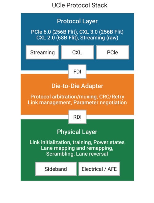
The UCIe stack consists of three layers. The top Protocol Layer ensures maximum efficiency and reduced latency through flow-control-unit-based (FLIT-based) protocol implementation, supporting the most popular protocols, including PCI Express® (PCIe®), Compute Express Link (CXL), and/or user-defined streaming protocols. The second layer is where the protocols are arbitrated and negotiated and where the link management occurs through a die-to-die adapter. The third layer, the PHY, specifies the electrical interface with the package media. This is where the electrical analog front end (AFE), transmitter and receiver, and sideband channel allow parameter exchange and negotiation between two dies. Logic PHY implements the link initialization, training and calibration algorithms, and test-and-repair functionality (see the figure).

Whether the primary goal is high-energy efficiency, high-edge usage efficiency, low latency, or all of the above, the UCIe specification has very competitive performance targets. To help you in your journey of adoption, Synopsys offers a complete UCIe Solution, allowing designers to put the specification into practice with PHY, controller, and verification IP (VIP).
The PHY interface supports both standard and advanced packaging options and is available in advanced FinFET processes for high-bandwidth, low-power, and low-latency die-to-die connectivity. The controller IP supports PCIe, CXL, and other widely used protocols for latency-optimized network-on-chip (NoC)-to NoC links with streaming protocols; for example, bridging to CXS interfaces and to AXI interfaces. Lastly, the Synopsys Verification IP (VIP) for UCIe supports various designs under test (DUT) at each layer of the full stack. The VIP includes testbench interfaces with/without PCIe/CXL protocol stack, Application Programming Interface (API) for sideband service requests, and API for traffic generation. Protocol checks and functional coverage are at each stack layer and signaling interface. It enables scalable architecture and Synopsys-defined interoperability test suites.
The Synopsys solution enables robust and reliable die-to-die links with testability features for known good dies and CRC or parity checks for error correction. It enables designers to build seamless interconnects between dies for the lowest latency and highest energy efficiency. With multi-die system designs, an increase in payloads due to multiple streaming protocols could take days or even months for simulations, limiting its usefulness.
To verify a multi-die system, designers can first create various single-node and multi-node models, simulating these minimalistic systems to check the integrity of data. Once those scenarios are tested, designers can then test in higher-level system scenarios with multi-protocol layers using the Synopsys ZeBu® emulation system, and then move to prototyping with the Synopsys HAPS® prototyping system. This flow from models to simulation to emulation to prototyping, using our verification IP and other protocol verification solutions, will help you ensure seamless interoperability pre-silicon.
Multi-die system design is a great option to catapult systems beyond the limitations of Moore’s law. With it, designers can realize new levels of efficiencies and performance while reducing power and area footprints. UCIe is helping to fast track this new way of designing for advanced applications. To learn more about how UCIe facilitates multi-die system designs, check out the Synopsys article, Multi-Die SoCs Gaining Strength with Introduction of UCIe.
For a list of UCIe compatible verification IP products, go to https://www.synopsys.com/verification/verification-ip.html, and for UCIe IP, go to https://www.synopsys.com/dw/ipdir.php?ds=dwc_ucie_ip.


Comments
There are no comments yet.
You must register or log in to view/post comments.