Electrical copper interconnects, once the backbone of data center networks, are facing growing challenges. Rapid expansion of AI and ML applications is driving a significant increase in cluster sizes within data centers, resulting in substantial demands for faster I/O capabilities. While the surge in I/O requirements is being addressed by faster SerDes PHY technologies, interconnects are facing scaling challenges from power consumption perspective. This coupled with the imperative to flatten networks to minimize latency is driving the trend to optical interconnects. Another reason for this shift is the ability of optical interconnects to reduce channel loss, thereby improving data transmission efficiency. Optical interconnects also address the rigidity and space limitations associated with copper cables, providing greater flexibility in designing and expanding data center architectures.
The Rise of Optical Interconnects
Optical data transfer over optical fiber with minimal loss (compared to copper cable) over longer distances has been in use for a long time. Optical interconnects are nothing new to the industry, but the current implementation approach uses traditional optical modules which consumes a lot of power. Consequently, there is a significant push to integrate optical components into semiconductor electronics. The goal is to enable faster data transmission over longer distances, at low latencies and reduced power consumption.
Silicon Photonics
Silicon photonics is a field that leverages the semiconductor manufacturing process to create optical components on silicon substrates. Integrating photonics on silicon offers numerous advantages but comes with its set of challenges. One major challenge is achieving efficient light generation, modulation and amplification on a silicon platform. Silicon, being an indirect bandgap material, is not suitable for generation of light. As a result, integration of direct bandgap materials is required, which can be complex and costly. Silicon photonics fabrication processes can vary from one foundry to another, some allowing monolithic integration of electronics and photonics on the same chip, while the others requiring co-packaging of electronic and photonic chips. Overcoming these challenges is crucial for realizing the full potential of silicon photonics in data centers.
OpenLight’s Integrated Photonic Integrated Circuits (PICs)
OpenLight has developed a technology to heterogeneously integrate indium phosphate (InP) on to a standard silicon process flow and create highly integrated devices. OpenLight’s PICs represent a significant advancement in the field of optical communication technology. These integrated circuits bring together a multitude of optical components, such as lasers, modulators, detectors, and waveguides, onto a single chip, offering a compact and highly efficient solution for data transmission and photonics applications. OpenLight’s Integrated PICs are engineered to meet the increasing demand for high-speed data transfer, lower power consumption, and enhanced performance. By consolidating these optical elements into a single package, OpenLight’s Integrated PICs facilitate seamless integration with electronic circuits, enabling more efficient and cost-effective solutions for data centers.
Synopsys and OpenLight Collaboration
Synopsys and OpenLight have collaborated to develop 100G/200G electro-optical interfaces that enable low power, low latency data centers. This electro-optical interface offers pluggable direct drive or linear or non-retimed interfaces. It enables data centers to choose high-speed connectivity options that suit their specific performance and power efficiency requirements, fostering flexibility and scalability in their network architecture.
Demo of 100G Electro-Optical Interface with TDECQ of 1.46dB
At the 2023 European Conference on Optical Communication (ECOC), Synopsys demonstrated its 112G Ethernet PHY IP Electrical-Optical-Electrical (E-O-E) interoperability success with OpenLight’s PIC. The eye diagram showed a TDECQ of 1.46dB, which is excellent. TDECQ stands for “Total Differential Eye Closure Quaternary,” a parameter used in optical communication systems to assess the quality of the received signal. TDECQ quantifies the amount of signal distortion or closure of the eye diagram in a digital communication system.
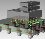
As shown in the block diagram below, the host PHY is driving the optical engine directly, avoiding the use of secondary PHY and DSP in the module. This approach is called linear drive or direct optical drive and leads to a 25% to 35% reduction in power consumption over a traditional optical module approach.
OpenLight recently unveiled the test results for the 200G Electro-Absorption-Modulator (EAM). This is a significant milestone toward enabling a 200G direct optical drive soon.
The Path to Success with Co-Simulation
The intricate interplay between optics and electronics requires seamless coordination to ensure optimal performance. One of the essential steps in harnessing the full potential of optical interconnects and high-speed SerDes is co-simulation. In a recent webinar, Synopsys emphasized the importance of co-simulation between optics and electronics and highlighted the comprehensive tool suite it offers to its customers.
Synopsys’ Photonic IC Design Solution
The Photonic IC Design Solution provides a suite of powerful design and simulation tools tailored for photonic devices. Engineers can create, analyze, and fine-tune a wide array of photonic components and circuits, including waveguides, modulators, detectors, and switches, with precision and accuracy. Its extensive library of pre-designed photonic building blocks, significantly expedites the design process by reducing the need to construct components from scratch.
The Synopsys solution promotes co-design, enabling seamless integration between electronic and photonic components. This ensures that both the electrical and optical aspects of a system are optimized for enhanced overall performance. Advanced simulation capabilities, including wave-optics and electromagnetic simulations, empower engineers to predict and understand the behavior of photonic components under varying conditions. Designers can iteratively refine their designs based on specific performance parameters like bandwidth, power consumption, and signal-to-noise ratio.
Synopsys’ OptSim
OptSim is a cutting-edge photonic system and circuit simulator designed to address the unique challenges and complexities of modeling and simulating photonic devices and systems. The simulator offers sophisticated optical modeling capabilities, enabling engineers to accurately model the behavior of light in various optical components and systems. OptSim seamlessly integrates with Synopsys’ electronic design automation (EDA) tools, allowing for co-simulation between photonic and electronic circuits.
Summary
As the demand for higher bandwidth and innovative data center architectures continues to surge, optical links are emerging as a pivotal solution. By embracing optical interconnects and leveraging high-speed SerDes solutions, data centers can achieve higher bandwidth, lower latency, more power-efficient data centers. The collaboration between Synopsys and OpenLight is leading the way in transforming data centers by harnessing the power of optical links. The successful EOE demonstrations substantiate the robustness of these next-gen optical link solutions. The emergence of standards-compliant technologies like 112G LR, VSR, XSR/Direct-drive, and the next-generation 224G is poised to revolutionize optical links, making them the ideal choice for 800G/1.6T data transmission. Co-simulation between optics and electronics is the key to unlocking the full potential of this transformative technology. Synopsys equips designers with a comprehensive set of tools to seamlessly implement, analyze, and verify their optical link designs.
For more details,
visit www.synopsys.com/ethernet
visit www.synopsys.com/photonic-solutions/optsim.html
Also Read:
Qualcomm Insights into Unreachability Analysis
Synopsys Panel Updates on the State of Multi-Die Systems
Synopsys – TSMC Collaboration Unleashes Innovation for TSMC OIP Ecosystem


