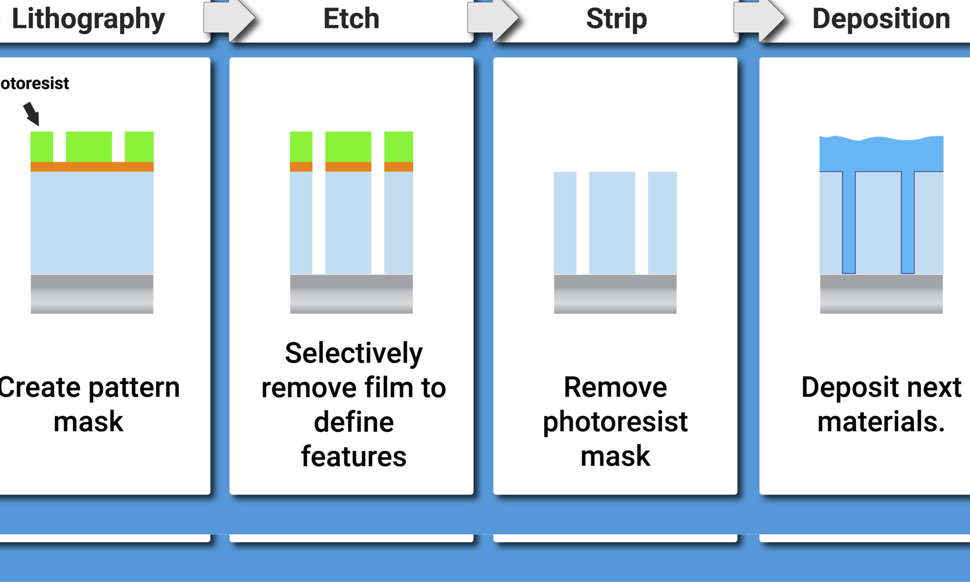

Readers of SemiWiki will be well aware of the challenges the industry has faced in photolithography in moving to new nodes, which drove the development of new EUV light sources as well as new masking techniques. Plasma etching is another key step in chip manufacturing that has also seen new challenges in the development of new sub-10nm processes.

Plasmas, the fourth state of matter, are formed by filling a vacuum chamber with a low-pressure gas and using electromagnetic energy inputs to ionize the gas: electrons are stripped from the ions and become unbound. Because electrons are more than a thousand times smaller than the ions, they move quickly relative to the ions. At the wafer surface, the electrons quickly strike the wafer and are depleted. A steady-state electric field known as the sheath is formed to balance the current losses. It is this boundary layer that gives the plasma many of its useful properties in manufacturing, such as plasma vapor deposition, plasma ashing (to remove the photoresist), or what we will focus on here, plasma etching. Plasma etching, also known as dry etching, was a breakthrough for achieving anisotropic etches for producing deep features. As seen below, the input gas type and volume, the applied voltage amplitude and waveforms, and the reactor geometry can all be varied to give considerable flexibility in plasma etching reactors. Common reactor types are capacitively coupled reactors, which use a single voltage source; reactive-ion etch (RIE) reactors, which have multiple electrodes to independently control the reactive ions for selective etching, or an inductively coupled plasma RIE (ICP-RIE) reactors, which use higher frequencies to enable higher densities and a faster etch rate. Designing a plasma etch reactor has a wide-range of input parameters to give a large design and operating space for solving a given manufacturing problem.

As the dimensions for semiconductor devices have become smaller, the implications for plasma etching have changed in multiple ways. Current advanced nodes have dramatically increased the film stack complexity for advanced logic. Other areas that will see increased challenges in scaling are the 3D NAND structures in advanced memory, or advanced packaging with its complex routing needs. For example, in the figure below, a schematic for a proposed RDL from Lau et.al.[1] is shown along with a scanning electron microscope image of the through-silicon via (TSV). This TSV, created using a Bosch-type Deep Reactive Ion Etch (DRIE), has an aspect ratio of 10.5 demonstrating the deep anisotropy capable of modern etch reactors. In these and other areas, the importance of being able to understand the details of the plasma etch has increased. For plasma etching, the critical issues are the degree of anisotropy (vertical etching versus horizontal etch), the shape of trenches (straight versus tapered or bowed as seen in the figure below) and etch uniformity. This is in addition to such traditional concerns such as etch rate and uniformity over the entire wafer that are critical for high yields and economics.
Controlling plasmas is difficult because they are complex chemically reactive gasses that interact with the semiconductor material in complex ways. Simulations have long been important in understanding plasma behavior in etch reactors. The three basic modeling paradigms are drift-diffusion, hydrodynamic (or fluid), and kinetic. These models are directly equivalent to the types of models used in modeling electron transport in TCAD algorithms for studying semiconductor devices. A key difference here is that the ions move instead of creating a solid-state lattice, and chemical reactions are also critical for understanding the plasma formation, properties, and etching abilities.
Drift-diffusion and fluid models are widely used to determine the overall energy balance and basic plasma properties. However, kinetic codes are critical for understanding the details of the plasma etching process. The degree of etch anisotropy is determined fundamentally by the energy and angle of ions as they strike the wafer, a quantity that is strongly dependent on the plasma sheath. The complexities of the sheath cannot be fully resolved with the drift-diffusion and fluid models, but require a kinetic code. Kinetic modeling is especially useful for gaining insights into the plasma uniformity, and degree of anisotropy of the etching process.
Tech-X Corporation has developed VSim, a kinetic modeling tool for simulating plasma etch reactors. Tech-X Corporation, located in Boulder, Colorado, has been in high performance computing in plasma physics for almost three decades. High-performance computing enables the details of ion and electron behavior to be computed across manufacturing-relevant spatial scales that are large relative to fundamental plasma length scales. With over a decade of experience in servicing the wafer equipment manufacturing market, Tech-X provides the leading plasma kinetic simulation capability. More information is here (http://www.txcorp.com/vsim) for VSim’s capabilities. In our next article, we will highlight enhancements for VSim 12 that will be released on September 14.
[1] Lau, J., et al. “Redistribution layers (RDLs) for 2.5 D/3D IC integration.” International Symposium on Microelectronics. Vol. 2013. No. 1. International Microelectronics Assembly and Packaging Society, 2013.
Also Read:
Coverage Analysis in Questa Visualizer
Fast EM/IR Analysis, a new EDA Category
DSP IP for High Performance Sensor Fusion on an Embedded Budget
Share this post via:


The Packaging PDK Is the Missing Layer for Co-Packaged Optics