For the first time ever, IEDM held a sustainability session at the 2023 conference. I was one of the authors who presented an invited paper, the following is a summary of my presentation.
Call to Action
From the United Nations [1]:
“Climate Change is the defining issue of our time, and we are at a defining moment.”
“Without drastic action today, adapting to these impacts in the future will be more difficult and costly.”
There are some basic well-established scientific links:
- The concentration of Greenhouse Gases (GHGs) in the earth’s atmosphere is directly linked to the average global temperature on Earth.
- The concentration has been rising steadily, and mean global temperatures along with it, since the time of the Industrial Revolution.
Two Part Problem
We view reducing GHG emissions as a two-part problem:
- Design future processes and technologies to reduce carbon emissions.
- But… we also need to reduce carbon emissions from existing facilities and processes.
Detailed modeling of carbon emissions is needed to understand both future process challenges and how to address existing processes/facilities.
Carbon Model
The Carbon Model described here is based on the former IC Knowledge Strategic Cost and Price Model that has been widely used in the industry since 2010. The Strategic Model is well vetted at this point. TechInsights acquired IC Knowledge in November 2022.
The Strategic Model – models 3D NAND, DRAM and Logic with coverage of the earliest processes on 300mm out to future processes. Currently the model covers 167 – 300mm fabs and 220 company specific process flows.
The model calculates detailed equipment sets with electric, water and natural gas requirements. Detailed materials consumptions by material type are also calculated.
The model is fab based! This is a key point when it comes to calibration and validation. There is a variety of GHG emissions data available, in some cases by company fab site, in some cases by country for a company, and in some cases for the whole company. The ability to model the fabs that make up a site, or all the fabs a company has in a country, or all the fabs a company has enables calibration and validation.
The Carbon Model is currently 300mm only although we are investigating adding additional wafer sizes. According to SEMI – 300mm represents roughly 70% of the worldwide millions of squares inches of silicon shipped in 2023.
The Carbon Model covers: GLOBALFOUNDRIES, Intel, Kioxia, Micron Technology, SK Hynix, Samsung, TSMC, and YMTC. These eight companies represent approximately 77% of worldwide 300mm wafer fab capacity [2]. We are investigating expanding the model coverage to all 300mm fabs.
In terms of GHG emissions the Carbon Model covers scope 1 emissions from on-site combustion of fossil fuels and process chemicals, and scope 2 emissions from purchased electricity (in a few cases electricity is generated on-site becoming a scope 1 emission).
Electricity Modeling
Some semiconductor companies are claiming they have no scope 2 electric emissions because they are using “100% renewable energy”. There are two problems with this.
- Renewable energy includes burning biomass that while considered renewable is not carbon free. This is not a significant part of electricity production in the countries we are interested in at this time, but back in 2015 Ireland produce >12% of their electric supply from burning peat [3].
- The far larger problem is that according to Greenpeace, in 2021, 84% of “Renewable Energy” in the semiconductor industry was from Renewable Energy Certificates (RECs) [4]. RECs are financial instruments that represent existing renewable energy projects. The purchase of RECs does not add any new renewable energy to the grid. For this reason, RECs are one of the least impactful forms of renewable energy procurement.
It is the modeling policy of TechInsights to not consider RECs and to model carbon emissions based on the carbon intensity of the electric supply. This is estimated by country except for US based fabs where we estimate it by state. We do account for carbon free electricity if generated on-site or through a purchase power agreement if we can identify it. That is an area of ongoing research for us.
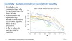
The past, present and projected carbon intensity by country we use in our modeling is illustrated in figure 1.
Figure 1. Carbon Intensity of Electricity by Country.
The solid lines are from Our World in Data and the dotted line projections are by applying an IEA projection by region that is no longer available on their web site.
In order to apply the carbon intensity, we need to first estimate the amount of electricity used by the fab. Because the Carbon Model does detailed equipment set modeling, we begin by applying electric usage by piece of equipment [5],[6],[7],[8]. EUV equipment gets particular attention due to the large effect dose has on throughput and therefore electric usage. Facility electric usage is estimated based on process and facility characteristics. Figure 2 illustrates electricity usage by logic node.
Figure 2. Electricity Usage by Logic Node.
In figure 2 the grey bars are facility electric usage, the blue bars are equipment electric usage not including EUV, the orange bars are 0.33NA EUV systems and the yellow-orange bars are 0.55NA (high NA) EUV system electric usage. The dotted line is the percentage of electric usage that is due to equipment.
There are three interesting aspects of the figure I want to highlight:
- The logic nodes in figure 2 are based on TSMC. At 7nm TSMC introduced an optical based process (7nm) and then an EUV based process (7nm+). Even though EUV equipment uses considerably more electricity than DUV systems, EUV replaces complex multi-patterning steps with a single exposure and results in a net reduction in electricity usage.
- At the 14A node we compared 0.33NA EUV that will require EUV multipatterning to 14A+ with High NA EUV eliminating multi-patterning and once again there is a net reduction in electricity usage.
- The dotted line shows that from 130nm to 40nm the equipment represented approximately 43% of total electric usage consistent with a SEMATECH study. Prior to EUV entering usage we found equipment represented 40% to 50% and then once EUV entered use equipment represent between 50% and 55% of total electricity consumption.
We have compared our modeled electricity usage to electric usage data for two companies – companywide (GF and SK Hynix), TSMC for Taiwan, and Intel for 4 sites and the match is excellent except for Intel Oregon where we believe we are underestimating the site activity level. Intel Oregon is a development site and we have recently received new data that is consistent with more activity there than we used in these calculations. Overall, it gives us confidence in the calculation.
Combustion
On site combustion of fossil fuels is for five applications:
- On-site electric generation (a few fabs do this with natural gas).
- Facility heat.
- Preheat water prior to reverse osmosis. Reverse osmosis is a key step in ultrapure water generation and the percentage of good water compared to reject water from reverse osmosis is higher if the water is warm.
- Some abatement systems – natural gas is used in some systems to burn perfluorinated compounds to destroy them.
- Heat and reheat, of makeup air. Wafer fabs have exhaust air to remove chemical fumes from equipment and air must be brought in from outside the facility to “make up” for the exhaust air. During cold weather the air must be heated to room temperature and humidified for static control and photoresist performance. During hot weather the makeup air is cooled below room temperature to dehumidify the air and then reheated to room temperature.
Process Chemicals
Figure 3 illustrates the flow of process gases through the process equipment and into the atmosphere with the conversion to equivalent carbon values.
Figure 3. Process Chemical Emissions.
From figure 3:
- Process chemicals enter the process chamber where some percentages are utilized either by being broken apart in an etch reaction or becoming part of a film in a deposition reaction. The initial input volume multiplied by 1-utilization is the amount of process chemicals in the exhaust.
- The process chamber exhaust may enter an abatement system where some portion of the process chemical is either broken down into non greenhouse gas chemicals or is absorbed into some medium. The chemicals exiting the abatement system is the input from the chamber exhaust multiplied by 1-abatement.
- Finally, the Global Warming Potential (GWP) is applied to convert the process chemical to carbon dioxide equivalents. Basically, the lifetime of the chemical and how much heat the chemical reflects back are combined to compare the effect of one gram of the chemical to one gram of carbon dioxide.
Figure 4 presents, utilization, abatement and GWP values for the chemicals of interest for wafer fabs.
Figure 4. Process Chemical Emissions Factors.
The utilization and abatement factors in figure 4 primarily come from the IPCC 2019 Refinement [9]. The GWP values are primarily from the IPCC AR5 [10].
The overall impact column in figure 4 is the 1-utilization values multiplied by the 1-abatement values multiplied by the GWP. This gives an overall picture of the impact of a chemical. Chemicals that have high overall impact are generally ones with high GWP values, however N2O has a relatively high impact despite a relatively low GWP. Most N2O is used for low temperature oxide-based film deposition with very low utilization [8] and the abatement is also relatively low.
Interestingly although the IPCC abatement values are generally over ninety percent, in the United States large greenhouse gas emitters must report their abatement efficiencies to the EPA and reported abatement values are much lower. Figure 5 illustrates reported abatement efficiencies for fabs sites in the US covered in the carbon model.
Figure 5. Reported Abatement Values for US Based Leading Edge 300mm Fabs.
It should be noted that the EPA reporting rules can result in reported abatement values that are less than actual abatement, but I would also note that when we model these fabs using the reported abatement values we get emissions consistent with what they report for emissions, so I don’t think the abatement values are very far off. I would also note I believe that abatement values are higher for fabs in some other countries and worldwide for the fabs covered in the carbon model I believe the average abatement is around 70%.
Model Validation
As was discussed in the Carbon Model section, the ability to model individual fabs can be used to compare the model calculated emissions to actual reported emissions.
In figure 6 EPA site emissions data from 4 sites representing 3 companies and 15 total fabs was added together and compared to modeled data for those same fabs.
Figure 6. Model Validation based on EPA Data for US Sites.
As can be seen from figure 6, the match by category is excellent. It should be noted that the match for the 4 sites in total is better than the match by individuals site.
The sites in figure 6 represent logic processes from 28nm down to 4nm.
In figure 7 the model is validated against total GHG emission by site, country or company.
Figure 7. Model Validation Against Company Reports.
In figure 7, Micron Singapore represents 3D NAND Fabs, Micron Japan and Taiwan are DRAM fabs, TSMC Taiwan is logic fabs, SK Hynix Company is 3D NAND and DRAM fabs, and Kioxia Yokkaichi is 3D NAND. The reported data in this plot comes from company ESG reports.
Once again, the match is excellent.
Model Results
Logic transistor density continues to increase although at a slower rate in the past, this is achieved by increasingly complex processes in terms of number of process steps and mask layers. 3D NAND bit density is increasing driven by increasing layers counts resulting in taller memory stack requiring more deposition and etching chemicals. DRAM bit density is also increasing although once again more slowly than in the past driven by increasing process steps and mask layers.
Figure 8 presents modeled emissions for logic, 3D NAND, and DRAM by “node”.
Figure 8. Modeled Emissions.
In figure 8, the logic emissions are presented for TSMC type logic processes run in Taiwan with 2023 Taiwan electric carbon footprint and 70% abatement efficiency. The 3D NAND and DRAM values presented are for Samsung processes run in South Korea with 2023 South Korea electric carbon footprint and 70% abatement.
For logic the biggest contributor is scope 2 electric carbon emissions, it should be noted that Taiwan has the highest carbon footprint electricity of any country where leading edge 300mm fabs are located. For 3D NAND the growing layer count/stack height drives increasing scope 1 process chemical and scope 2 electric usage. For DRAM scope 2 electric emissions are the largest source of carbon emissions until a projected 3D DRAM process is introduced. The 3D DRAM process has a very tall memory stack requiring a lot of deposition and etch chemical usage.
There are multiple opportunities to dramatically reduce carbon emissions:
- Scope 2 electric emissions can be reduced by switching to low carbon emissions electricity sources such as wind, nuclear, hydro, or solar.
- Abatement systems with up to 99% abatement efficiency are available [11].
- Lower carbon emission process chemistries can be substituted for existing higher emission chemistries. At the VLSI Technology conference this year Tokyo Electron disclosed a cryogenic etcher that can etch 3D NAND stacks with non GHG chemistries and higher etch rates. Also, chamber cleaning is typically done with SF6 or NF3 acting as fluorine delivery vehicles. Both gases have high GHG GWP values. In place of SF6 and NF3, F2 with a GWP of 0 or COF2 with a GWP of 1 can be substituted. It should be noted that even though these gases have 0 or 1 for a GWP they can combine with other species in the chamber to produce a high GWP molecule.
Figure 9 presents emissions in 2030 based on three scenarios each for a 10A logic process, a 1,000 layer 3D NAND process and a 80 layer 3D DRAM process.
Figure 9. Carbon Footprint 2030.
In each case the 2023 value is assuming 2023 electricity carbon footprint and 70% abatement with current process chemistries. The 2023 – likely scenario is based on the projected 2030 electricity carbon footprints from figure 1, 90% abatement and a new memory etch system/chemistry. Finally, 2030 – possible is based on 24g CO2 equivalent per kilowatt hour electricity (solar is 48, Hydro 24, wind and nuclear are 12 [5]).
Conclusion
The TechInsights Carbon model has been developed based on the former IC Knowledge Strategic Cost and Price Model. The carbon model enables detailed comparison of 300mm fabrication for leading-edge companies. Electric sources, combustion, and process chemicals with utilization, abatement, and GWP are all modeled. The carbon model includes extensive company specific data. The carbon model is currently available from TechInsights.
References
[1] https://www.un.org/en/global-issues/climate-change
[2] TechInsights 300mm Watch Database.
[3] https://www.seai.ie/data-and-insights/seai-statistics/key-statistics/electricity/
[4] Invisible Emissions: A forecast of tech supply chain emissions and electricity consumption by 2030,” Greenpeace.
[5] Bardon, et.al., “DTCO including Sustainability: Power-Performance-Area-Cost-Environmental score (PPACE) Analysis for Logic Technologies,” IEDM (2020).
[6] ASML 2022 annual report, page 83.
[7] Smeets, et.al., “0.33 NA EUV systems for High Volume Manufacturing,” SPIE (2022)
[8] TechInsights
[9] https://www.ipcc-nggip.iges.or.jp/public/2019rf/pdf/3_Volume3/19R_V3_Ch06_Electronics.pdf
[10] https://www.ipcc.ch/report/ar5/wg1/
[11] https://www.ebara.co.jp/en/products/details/FDS.html
Also Read:
Seven Silicon Catalyst Companies to Exhibit at CES, the Most Powerful Tech Event in the World
RISC-V Summit Buzz – Launchpad Showcase Highlights Smaller Company Innovation