The performance demands of data centers continue to grow, driven to large degree by the ubiquitous use of complex AI algorithms. On April 25, Embedded Computing Design held an informative webinar on this topic. Two experts looked at the problem from the standpoint of processor architecture and communication strategies, which covers a lot of ground. It turns out AI can be used to solve some of the challenges of bringing AI algorithms to life. A link for the replay is coming, but first, let’s look at the topics covered as Samtec and Achronix expand AI in the data center.
Webinar Background
The event was part of Embedded Computing Design’s An Engineer’s Guide to AI Integration webinar series. According to the publication:
AI is one of the most complex technologies embedded developers must tackle. Integrating it into your system brings with it so many questions and not so many answers. In this monthly series, Embedded Computing Design will look to simplify the design process, as much as that’s possible.
In this webinar, the differences between data center design and conventional embedded computer design were examined, with a look at what choices a developer needs to make. The presenters were:
Matt Burns
Global Director, Technical Marketing, Samtec
Viswateja Nemani
Product Manager of AI & Software at Achronix
And the moderator was:
Rich Nass
Executive Vice-President, Brand Director, Embedded Franchise, OpenSystems Media
Rich brought a lot of knowledge and perspective to the event and did a great job moderating the webinar and conducting a valuable Q&A session afterwards. The presenters also brought a lot to the event. Samtec’s Matt Burns and Achronix’s Viswa Nemani have extensive knowledge of AI algorithms and the demands they bring to system design.
Samtec covers a broad range of high-performance communication technology and Achronix covers a broad range of high-performance computing technology. This combination makes for a complete view of the challenges data center and system designers face. You can learn more on SemiWiki about Samtec here, and Achronix here.
The Achronix FPGA-Powered View
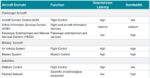
Viswa kicked off the discussion by explaining of how the various layers of AI algorithms relate to each other and how each delivers unique capabilities. The diagram below summarizes this discussion; it is useful to understand how AI builds upon itself.
He then framed how data centers fit and what challenges exist. Viswa explained that data centers are uniquely positioned to support AI applications thanks to the connectivity and processing power they deliver. He pointed out that vast amounts of data pass through today’s data centers, requiring huge storage and compute capabilities. The AI workloads running in data centers demand high power densities, requiring as much as 100kW+ per cabinet and liquid cooling. This is the beginning of the design challenges.
He explained that AI/ML algorithms are exceptional at spotting patterns in data. This leads to opportunities to improve efficiency, implement predictive and prescriptive analytics, optimize energy, reduce cost, and enhance security and productivity. Viswa then went into detail on each of these topics. It is a very useful and relevant discussion.
He outlined the many benefits of FPGAs play in data center architecture:
- Real-time processing
- Low latency, e.g., Automatic speech recognition
- Efficiency
- Increase performance and energy efficiency of existing systems through accelerators
- React quickly
- To new market opportunities and competitive threats using programmable accelerators
- Operational agility
- Host and scale multiple applications on a single heterogeneous platform
- Rapid deployment of new applications while minimizing total cost of ownership
- In-network compute
- Processing as traffic moves
Viswa concluded by discussing the Achronix Speedster7t FPGA and its ways of delivering enhanced performance, lower cost and faster time-to-market. Some very compelling information shared here. He also discussed Achronix embedded FPGA (eFPGA) IP and accelerator cards. Watch the full webinar now.
The Samtec View
Matt also began his discussion with an overview of AI algorithms. In this case, he discussed the evolution of high-profile AI applications. One example he cited was the move from OpenAI’s ChatGPT to its new application, Sora. ChatGPT will create textual answers to textual questions while Sora will create images from textual descriptions. These new breakthroughs in large language models increase performance and power demands exponentially. Both Viswa and Matt cite some sobering statistics about these increases.
While this all seems like a huge problem, Matt explained how much more is coming. Early AI models from around 2018 had about 100 million parameters (ELMo is the example he cited). Today, LLM models such as ChatGPT have about 100 – 200 billion parameters just six years later. And the latest models require about 1.6 trillion parameters. The “tip of the iceberg” moment came when Matt pointed out that a human of average intelligence has about 100 trillion synapses. If we’re going after human-like intelligence, we have a long way to go.
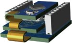
With this backdrop of continued exponential growth in processing capability (and associated power consumption), Matt began a discussion of how to route all that data between the huge number of processing elements involved. Solving this problem is a core strength of Samtec, and Matt spent some time explaining the capabilities the company brings to a broad class of high-performance computing designs.
Matt discussed what Samtec offers from the front panel to the backplane for data center designs. The photo below summarizes some of the latest silicon-to-silicon connectivity solutions Samtec offers.
This large catalog of technologies can optimize data routing electrically, optically or via RF. Couple these cutting-edge products with expert design support and highly accurate, verified models and you can begin to see how Samtec is the perfect partner to address the continued exponential demands that AI will create.
Matt discussed a couple of AI-related applications to help put things in perspective. First, he discussed the special requirements of AI accelerators. He touched on the many new specifications that must be addressed (e.g., PCIe® and CXL®). He also discussed the need for domain specific architectures that are needed to support new hardware Al chipsets that create complete end-to-end Al systems. This level of innovation is required as current compute density is insufficient to address the demands of newer AI models. Nvidia Blackwell was used as an example.
Matt described many solutions from Samtec to address these trends, from high-performance connectors, cables to direct chip attach solutions. These solutions deliver superior performance and density when compared to traditional PCBs alone.
The breadth of capabilities Matt described is quite complete and compelling. You can explore Samtec’s AI solutions here. You will find a lot of product information there, as well as a very useful white paper called Artificial Intelligence Solutions Guide.
The webinar ended with a very informative Q&A session moderated by Rich Nass.
To Learn More
By now, you should really want to watch this webinar. If AI architectures are part of your future, it’s a must-see event. You can access the webinar replay here. This will help you to really understand how Samtec and Achronix expand AI in the data center.