From humble beginnings in military applications, the semiconductor industry has been fundamental to all societal growth, and everything that grows exponentially depends on semiconductors.
It is not a gentle industry. Products over two years old are unsellable, and there is either too much supply or none. Semiconductor scarcity can kill companies faster than anything else, and components bought at the wrong price can make a product unsellable.
Thanks for reading Semiconductor Business Intelligence! Subscribe for free to receive new posts and support my work.
While the industry’s supply channels are incredibly complex, they are also the key to understanding what is happening. A change somewhere in the supply network causes ripples that move backwards and forwards in the network. Because of these propagations, you can predict what will happen in other areas of the supply network, and you can peek into the future.
Your future might be somebody else’s past
The first question in all strategy development is, “What is going on?” We make a living by dissecting the industry and its supply chain and providing strategic input to our clients.
Of course, you can join all the stock analysts at the investor calls and hear the Charismatic Earnings Overpromiser (CEO) tell you what’s really going on! We are still on the calls, but we know everybody had a good quarter and gained market share. We check the blah-blah through analysis. It is not always right, but it is always neutral and independent.
All Semiconductor companies had a great quarter and gained market share!
No—it does not start with a grain of sand! It begins with a tool. Some tools are more advanced than any other manmade object and constantly evolve. From a quiet existence in the university cities of Northern Europe, they are now vital assets in the geopolitical chess game between China and the Western world.
This makes analysing the Semiconductor Tools market one of the most exciting things we do (we don’t have a life).
The key companies in the tool market
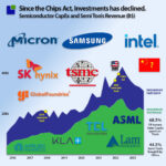
Contrary to what should be expected when listening to all the noise about semiconductor subsidies, grants, and new factories being built, the revenue for tools is not growing. That is not to say it will not happen, only that it is unexpected. Also, the US is trying to regain chip manufacturing supremacy in the most advanced logic nodes; you should expect growth from ASML, which delivers the most advanced lithography tools for the industry.
The opposite is happening right now, with ASML revenue declining by almost 30% while its largest competitor, Tokyo Electron, grew 17%.
AMAT, the leading deposition Company, returned as the most prominent tool company in Q1-2024, with a 23% market share.
While the Chips Act and subsidies undoubtedly will eventually impact tool sales, it has not happened yet. The target of the Subsidies is independence from Chinese influence, be it military or economic. Still, the Chinese are not sitting with their hands in their laps while money is being distributed in the West.
Since the US Chips Act was signed, overall tool sales have decreased while tool sales to China have increased. China now buys nearly 45% of the tools the top Western Tool manufacturers sell.
The Chips Act has substantially impacted tool sales, although not in the expected direction. Significantly lower tool sales to the USA, Taiwan, and Korea have been recorded, while China’s appetite for Western Semiconductor tools has increased.
It is estimated that 75% of all Capital Expenditures (CapEx) associated with the construction of fabs are Tool expenses, with Lithography tools accounting for the largest share of the costs.
Below is an overview of CapEx spending for the large Semiconductor Fab owners. CapEx crossed $40B$ a quarter just after the Chips Act was signed but has been declining ever since. Not surprisingly, Tools revenue follows the CapEx development with two interesting deviations:
- Tools take a larger share of CapEx over time
- Except after the Chips Act was signed.
Undoubtedly, the Chips Act and other subsidies drive this change but not in the expected direction. We are not trying to imply that the Chips Act will not significantly impact the US Semiconductor Industry other than saying it might have some unintended side effects.
First, the Chips Act has changed the timing of Semiconductor investments as much as it has impacted their location.
Second, it has changed what CapEx is spent on. Greatly simplified, the Semiconductor factory owners spend the big money on four activities:
As semiconductor equipment is delicate and ages quickly, a significant amount of CapEx is spent on maintenance and one-for-one replacements to prevent capacity decline. Memory companies failed to do this during the downturn.
Right now, the Semiconductor fab owners have down-prioritised upgrading the existing factories to get subsidies. The US government and others want you to place your big box in their backyard to access the candy jar.
Currently, there is ample capacity outside memory and the smallest logic nodes, but we are early in the Semiconductor cycle. We are tinkering with the supply-demand equation, which can dramatically affect the industry. Soon, we will be capacity-constrained again, and this time around, we will not have built the capacity through upgrade activities. It could become nasty with potential AI upgrade cycles of PCs and Smartphones.
And suddenly, all of the capacity from the subsidies will come online at the beginning of 2026, creating a potential Mother of all Semiconductor cycles.
But what about China?
All this money-spraying was about stopping the Chinese attempt to dominate the Semiconductor Industry. This has been happening for decades since the Chinese authorities understood that the value was not in assembly but locked in the assembled semiconductors. Significant investments have been made, but it proved more difficult than expected.
As geopolitical tensions increased, the Chinese authorities shifted focus from building Semiconductor manufacturing capacity to investing in Semiconductor tools, as the most advanced equipment was embargoed.
Even though the Chinese semiconductor tools industry was small compared to Western manufacturers, it grew at an astonishing rate of nearly 50% CAGR until it reached above $2B in the last quarter of 2023.
Growth stopped in Q1-24—the decline of 21.9% is more than can be explained by the Chinese New Year. This can be seen by comparing this year’s holiday effects to the prior year’s.
It looks like congestion in the supply chain. Fortunately, our little box of numbers can add flavour to the discussion.
The Chinese Tool Manufacturers have grown rapidly but also amassed enormous inventory.
Closing in on three years of inventory is significant, especially if demand is collapsing.
Through production unit statistics, we can get some insights into the local demand in China. As can be seen, most of the significant Semiconductor products are not growing as rapidly as before. Combined, they have been flat over the last year.
Except for manufacturing of semiconductors. A massive 44.6% growth from a year ago supplying a market that is virtually flat.
The Chinese are not flooding the western markets with cheap products because they want to – it is because they need to. The Chinese semiconductor market is in complete oversupply.
The Chinese is already struggling with tariffs that where just made worse by the Biden Administration this week. Semiconductor tariffs will increase from 25% to 50% and electrical cars will bee slapped with a 100% tariff. This will not make the oversupply in China easier.
As you have seen, there is a lot going on in the market right now and it will be difficult to accurately predict what strategic decisions will prove to be right. We will keep monitoring all the supply pipes looking for hot water and leaks.
Should you be interested in using our research for your strategy development, please do not hesitate to contact us here.
We hope you have enjoyed our data story on the Semiconductor Tools market and our insights will help you make decisions. We would appreciate a like or a comments on our work.
As our insights are not the only insights that can be driven, feel free to add to the discussion if you have knowledge and insights that can add flavour to the discussion.
Also Read:
Oops, we did it again! Memory Companies Investment Strategy