You are currently viewing SemiWiki as a guest which gives you limited access to the site. To view blog comments and experience other SemiWiki features you must be a registered member. Registration is fast, simple, and absolutely free so please,
join our community today!
Last week I attended the SPIE Advanced Technology Conference. There were a lot of interesting papers and as is always the case at these conferences, there was a lot of interesting things to learn from talking to other attendees on the conference floor.
The first interesting information from the conference floor was that 450mm is… Read More
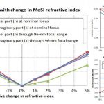
Let’s start with the bottom line: in 14nm processes, errors which have typically been little more than noise with respect to photomask critical dimension (CD) control targets at larger process nodes are about to become very significant, even out of control if not accounted for.… Read More
The industry plans to use 193nm light at the 20nm, 14nm, and 10nm nodes. Amazing, no? There is no magic wand; scientists have been hard at work developing computational lithography techniques that can pull one more rabbit out of the optical lithography hat.
Tortured metaphors aside, the goal for the post-tapeout flow is the same… Read More
While the SPIE Advanced Lithography conference is best known for IC manufacturing, computational lithography, mask preparation and other back-end topics, there is also a significant amount of interest in Design for Manufacturing (DFM) at the conference because some litho issues are best (or only) addressed by modifying the… Read More
As part of the DFM Conference at the SPIE Advance Lithography symposium, the DFM committee is conducting an informal survey on the current state of Design For Manufacturability in the Semiconductor Industry.
Please take this anonymous 16 question survey to identify critical Design for Manufacturability (DFM) issues facing… Read More