As the leading global lithography event, the technical program will focus on works in optical lithography, metrology, and EUV. Leaders come to solve challenges in lithography, patterning technologies, and unique materials, while sharing the latest advancements in the semiconductor industry.
Browse papers in the program.… Read More
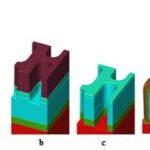
As feature sizes have shrunk, the semiconductor industry has moved from simple, single-exposure lithography solutions to increasingly complex resolution-enhancement techniques and multi-patterning. Where the design on a mask once matched the image that would be produced on the wafer, today the mask and resulting image … Read More
The annual SPIE Advanced Lithography Conference kicked off last night with vendor sponsored networking events and such. SPIE is the international society for optics and photonics but this year SPIE Advanced Lithography is all about the highly anticipated EUV technology. Scotten Jones and I are at SPIE so expect more detailed… Read More
As I write about integrated photonics I continue to hear from long-time experts in the field who lament that integrated photonics has been around for decades and other than telecom/datacom, it seems to never be a mainstream technology. It’s hard to argue that this time around it will be different as those people have lived through… Read More
For me personally EUV has been something of a roller coaster ride over the last several years. I started out a strong believer in EUV but then at the SPIE Advanced Lithography Conference in 2014 TSMC gave a very negative assessment of EUV, and there was a SEMATECH paper on high NA EUV that struck me as extremely unlikely to succeed. I … Read More
I have previously written about SPIE day 1 and 2 so I want to wrap up my coverage with some impressions from days 3 and 4. My single biggest take away from the conference is that EUV has made tremendous progress in the last 12 months. Last year the mood of the conference was in my opinion pessimistic with respect to EUV, this year the mood… Read More
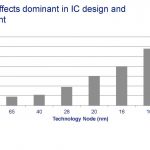
With today’s ArF based lithography using 193nm wavelength light, we are hard up against the limitations imposed by the Raleigh equation. Numerous clever things have been devised to maximize yield and reduce feature size. These include 2 beam lithography, multiple patterning, immersion litho processes to improve NA, thinner… Read More
Next week is the SPIE Advanced Lithography Conference in San Jose, the premier conference for advanced lithography used to produce state-of-the-art semiconductors. Last year I blogged after the conference about some of the key points I heard at the conference and this year I plan to do the same.
Last year’s blog is available HERE… Read More
The 40[SUP]th[/SUP] SPIE Advanced Lithography conference will be at the San Jose Convention Center 22-26 February. Over the past few years, this conference has grown in scope to include emerging patterning technologies, like directed self-assembly (DSA) and design-process-technology co-optimization.
Underlying all … Read More
I spent all of last week at SEMICON West meeting with customers, potential customers, partners and various industry analysts and experts. I was involved in many interesting discussions over the course of the week and I thought I would share some of the more interesting observations:
Alternate Fin Materials Pushed Out
I have for… Read More