You are currently viewing SemiWiki as a guest which gives you limited access to the site. To view blog comments and experience other SemiWiki features you must be a registered member. Registration is fast, simple, and absolutely free so please,
join our community today!
One of the great pleasures in what I do is to work with people who are working with people in some of the hottest design areas today. A second-level indirect to be sure but that gives me the luxury of taking a broad view. A recent discussion I had with Kurt Shuler (VP Marketing at Arteris IP) is in this class. As a conscientious marketing… Read More
One of the key growth areas for the semiconductor ecosystem is IP which of course includes IP related EDA software. In May of 2017 design management/collaboration expert (one of my personal favorite EDA companies) ClioSoft announced designHUB[SUP]®[/SUP] for IP management and re-use. Using designHUB, semiconductor companies… Read More
I think Synopsys would agree that they were not an early entrant to the emulation game, but once they really got moving, they’ve been working hard to catch up and even overtake in some areas. A recent webinar highlighted work they have been doing to overcome a common challenge in this area. Being able to boot a billion-gate design, … Read More
EDA is big on growth through acquisition, being acquired many times throughout my career I know this by experience. In fact, we have a wiki that tracks EDA Mergers and Acquisitions and it is the most viewed wiki on SemiWiki.com with 101,918 views thus far.
In March of 2017 ANSYS acquired CLK Design Automation which did timing variation… Read More
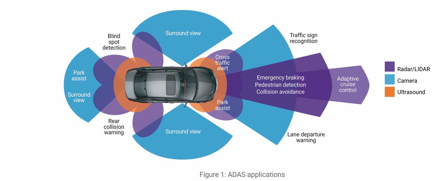
No area of electronics is moving faster than automotive semiconductors. Everyone has been talking about the increasing electronics content of automobiles for decades. With Advanced Driver Assistance System (ADAS) and autonomous driving becoming a reality the pace has picked up even more. These new designs combine just about… Read More
A recent press release from eSilicon caught my eye. The company has been touting their 7nm SerDes quite a bit lately – reach, power, flexibility, things like that. While those capabilities are important, any high-performance chip needs to work in the context of the system, which usually contains technology from multiple sources.… Read More
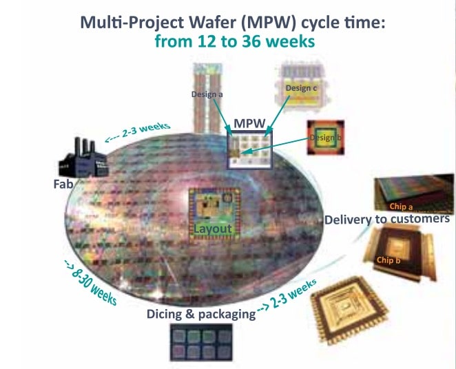
On SemiWiki we often talk about bleeding-edge technology like 7nm, 5nm or even 3nm, but for analog IC designs there’s a low-cost alternative to getting your ideas validated and prototyped without taking out a multi-million dollar loan, and that’s through the use of Multi-Project Wafers (MPW). Starting with a mature… Read More
Lyft’s S1 filing for its IPO is a sobering read, as such documents often are, requiring, as they do, the full disclosure of current financial circumstances and, everyone’s favorite: risk factors. Lyft identifies 18 risk factors (below) which could interfere with the long-term success of the operation. I think there are more.… Read More
Webinars are a quick way to come up to speed with emerging trends in our semiconductor world, so I just finished watching an interesting one from Moortec about the benefits of embedded in-chip monitoring for Data Center and AIchip design. My first exposure to a data center was back in the 1960s during an elementary school class where… Read More
Arm announced their Neoverse plans not long ago at TechCon 2018. Neoverse is a brand, launched by Arm, to provide the foundations for cloud to edge infrastructure in support of their vision of a trillion edge devices. To a cynic this might sound like marketing hype. Sure, they’re widely used in communications infrastructure and… Read More


Should Intel be Split in Half?