

On SemiWiki we often talk about bleeding-edge technology like 7nm, 5nm or even 3nm, but for analog IC designs there’s a low-cost alternative to getting your ideas validated and prototyped without taking out a multi-million dollar loan, and that’s through the use of Multi-Project Wafers (MPW). Starting with a mature process node like 180nm still produces adequate silicon for low-power applications like IoT where analog sensors and converters are the main part of the chip functionality, along with some digital control logic, think big A and little D applications.
My industry contact Wladek Grabinski shared information with me this week about a company in France called CMP(English translation Multi-Project Circuits) that has been offering MPW foundry services since 1981 to keep costs down for IC designers at Universities, research laboratories or industrial companies that want to prototype their analog ideas economically.
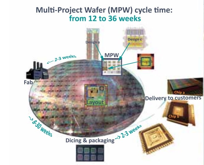
For an MPW project you likely want from dozens to thousands of pieces manufactured for you, either packaged or just bare die, ready for testing. In total, some 7,900 projects have been prototyped through 1,043 MPW runs at CMP over the years, helping 614 customers realize their analog ideas into silicon. CMP certainly has their act together and provide a much needed service for companies needing to get quick prototypes for big A, little D designs.
A Swiss company em microelectronic (EM) has an ultra low-power IP library and foundry all ready to use with MPW services provided by CMP. Here’s what EM has to offer you:
- Mature 180nm node for ultra low-power analog design (APL018)
- NVM (EE or Flash)
- EKV accurate models near and sub Vth operation
- Analog and digital IP libraries characterized for low voltage (down to 0.4V), low current (nA bias)
- I/O pads, low leakage ESD protection
- Design Kit for Cadence
- Digital flow for Synopsys
EM really knows IC design, as they’ve been in business since 1975 and their ultra-low power silicon is used in six major application areas:
- Energy – harvesting, power management, storage
- Interfaces – displays, tactile surfaces, computer peripherals, motion sensing, sound production
- Sensing – interfaces, sensors
- Communications – RF technologies, RF long range communication, RFID, beacons
- Smart Processing – wearables, cryptography and security
- Time – watches, fobs
Even though the EM headquarters are in Marin, Switzerland, you can also find their facilities around the globe in:
- Colorado Springs, USA
- Prague, Czech Republic
- Bangkok, Thailand
If you’ve ever shopped for a watch you likely have seen the iconic Swatch brand in retail stores and online, so EM is the semiconductor company for Swatch.

Looking at the most recent press releases at EM I conclude that this company is well suited for IC designs that require Bluetooth, IoT, RF and anything that is battery-powered and requires ultra-low power consumption.
CMP invited EM to present at a seminar last month, so check out the slides here.
Share this post via:


The Packaging PDK Is the Missing Layer for Co-Packaged Optics