You are currently viewing SemiWiki as a guest which gives you limited access to the site. To view blog comments and experience other SemiWiki features you must be a registered member. Registration is fast, simple, and absolutely free so please,
join our community today!
WP_Term Object
(
    [term_id] => 158
    [name] => Foundries
    [slug] => semiconductor-manufacturers
    [term_group] => 0
    [term_taxonomy_id] => 158
    [taxonomy] => category
    [description] =>
    [parent] => 0
    [count] => 1364
    [filter] => raw
    [cat_ID] => 158
    [category_count] => 1364
    [category_description] =>
    [cat_name] => Foundries
    [category_nicename] => semiconductor-manufacturers
    [category_parent] => 0
    [is_post] =>
)
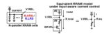
Resistive RAM (ReRAM) technology has emerged as an attractive alternative to embedded flash memory storage at advanced nodes. Indeed, multiple foundries are offering ReRAM IP arrays at 40nm nodes, and below.
ReRAM has very attractive characteristics, with one significant limitation:
- nonvolatile
- long retention time
- extremely
…
Read More
Now that semiconductor conferences are virtual there are better speakers since they can prerecord and we have the extra time to do a better job of coverage. Even when conferences go live again I think they will also be virtual (hybrid) so our in depth coverage will continue.
ISSCC is one of the conferences we covered live since it’s… Read More
GF has played some groundbreaking roles in the semiconductor ecosystem. The spinout of the AMD fabs and the acquisition of the IBM semiconductor division just to name two. Another big one would be the GF Initial Public Offering which may come as early as 2022.
When the IPO was first mentioned during a chat with GF CEO Tom Caulfield … Read More
Intel is a semiconductor legend. Founded on July 18, 1968, the name Intel is short for Integrated Electronics. After leading Silicon Valley, the United Sates, and the world into the era of semiconductors through technical excellence, Intel has hit some challenging times. There has been quite a bit of CEO drama that we will look … Read More
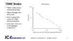
There is a lot of interest right now in how Intel compares to the leading foundries and what the future may hold.
Several years ago, I published several extremely popular articles converting processes from various companies to “Equivalent Nodes” (EN). Nodes were at one time based on actual physical features of processes but had… Read More
We have seen that the interface IP category is seeing incredibly high growth rate over the last two decades and we expect this category to generate an ongoing high source of IP revenues for at least another decade. But if we dig into the various successful protocols like PCI Express, Ethernet or USB, we can detect a common function … Read More
-KLAC- Solid QTR & Guide but flat 2021 outlook
-Display down & more memory mix
-KLAC has very solid Dec Qtr & guide but 2021 looks flattish
-Mix shift to memory doesn’t help- Display weakness
-Despite flat still looking at double digit growth
-EUV driven business may see some slowing from digestion
As always, … Read More
-Intel good results had a little extra help to be great
-New CEO commits to remaining an IDM versus fabless
-Claims of strong progress on 7NM fuel optimism inside
-Outsourcing to TSMC will not go away but will increase
A good quarter but with some silicon enhancements from ICAP
Intel reported Revenues of $20B and EPS of $1.52, which… Read More
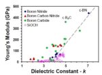
Of the three types of materials used in microelectronics – i.e., semiconductors, metals, and dielectrics – the first two often get the most attention. Yet, there is a pressing need for a rich variety of dielectric materials in device fabrication and interconnect isolation to satisfy the performance, power, and reliability … Read More
Spin-transfer torque magnetoresistive RAM (STT-MRAM) has emerged from several foundries as a very attractive IP option. An introduction to MRAM technology from GLOBALFOUNDRIES was provided in this earlier SemiWiki article. [1]
Briefly, STT-MRAM is a non-volatile storage option with the following attractive characteristics… Read More


Musk’s Orbital Compute Vision: TERAFAB and the End of the Terrestrial Data Center