You are currently viewing SemiWiki as a guest which gives you limited access to the site. To view blog comments and experience other SemiWiki features you must be a registered member. Registration is fast, simple, and absolutely free so please,
join our community today!
WP_Term Object
(
    [term_id] => 158
    [name] => Semiconductor
    [slug] => semiconductor-manufacturers
    [term_group] => 0
    [term_taxonomy_id] => 158
    [taxonomy] => category
    [description] =>
    [parent] => 0
    [count] => 1403
    [filter] => raw
    [cat_ID] => 158
    [category_count] => 1403
    [category_description] =>
    [cat_name] => Semiconductor
    [category_nicename] => semiconductor-manufacturers
    [category_parent] => 0
    [is_post] =>
)
In 2020 TSMC established its Net Zero Project with a goal of net zero emissions by 2050. I remember wondering how could this possibly be done before 2050 or at all for that matter. After working with TSMC for 20+ years I have learned never to bet against them on any topic and green manufacturing is one of them, absolutely.
TSMC presented… Read More
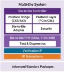
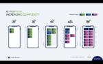
For decades now I’ve watched the incredible growth of SoCs in terms of die size, transistor count, frequency and complexity. Instead of placing all of the system complexity into a single, monolithic chip, there are now compelling reasons to use a multi-chip approach, like when the maximum die size limit is reached, or it’s… Read More
There were quite a few announcements at the TSMC Technical Symposium last week but the most important, in my opinion, were based on TSMC N3 tape-outs. Not only is N3 the leading 3nm process it is the only one in mass production which is why all of the top tier semiconductor companies are using it. TSMC N3 will be the most successful node… Read More
TSMC also covered manufacturing excellence. The TSMC “Trusted Foundry” tagline has many aspects to it, but manufacturing is a critical one. TSMC is the foundry capacity leader but there is a lot more to manufacturing as you will read here. Which brings us to the manufacturing accomplishments from the briefing:
To
…
Read More
TSMC covered their specialty technologies in great detail. Specialty is what we inside the ecosystem used to call weird stuff meaning non-mainstream and fairly difficult to do on leading edge processes. Specialty technologies will play an even more important part of semiconductor design with the advent of chiplets where die… Read More
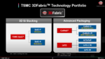
TSMC’s 3DFabric initiative was a big focus at the symposium, as it should be. I remember when TSMC first went public with CoWos the semiconductor ecosystem, including yours truly, let out a collective sigh wondering why TSMC is venturing into the comparatively low margin world of packaging. Now we know why and it is absolutely… Read More
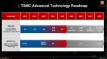
The next topic I would like to cover is an update to the TSMC process node roadmap starting with N3. As predicted, N3 will be the most successful node in the TSMC FinFET family. The first version of N3 went into production at the end of last year (Apple) and will roll out with other customers in 2023. There is a reported record amount of … Read More
The TSMC 2023 North America Technology Symposium happened today so I wanted to start writing about it as there is a lot to cover. I will do summaries and other bloggers will do more in-depth coverage on the technology side in the coming weeks. Having worked in the fabless semiconductor ecosystem the majority of my 40 year semiconductor… Read More
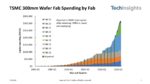
Up until November of 2022, IC Knowledge LLC was an independent company and had become the world leader in cost and price modeling of semiconductors. In November 2022 TechInsights acquired IC Knowledge LLC and IC Knowledge LLC is now a TechInsights company.
For many years, IC Knowledge has published a database tracking all the 300mm… Read More
Mobile World Congress (MWC) is the world’s largest gathering of mobile industry innovators where one can hear the latest on advanced technologies and solutions. This year, it took place from February 27 through March 2. Soitec was there to share their insights on how mobile communications are going to evolve with 5G and beyond … Read More

TSMC CoWoS versus Intel EMIB Semiconductor Packaging