It is quite amazing that silicon-based devices have been the foundation of our industry for over 60 years, as it was clear that the initial germanium-based devices would be difficult to integrate at a larger scale. (GaAs devices have also developed a unique microelectronics market segment.) More recently, it is also rather amazing that silicon field-effect devices have found a new life, through the introduction of topologies such as FinFETs, and soon, as nanosheets. Research is ongoing to bring silicon-based complementary FET (CFET) designs to production status, where nMOS and pMOS devices are fabricated vertically, eliminating the lateral n-to-p spacing in current cell designs. Additionally, materials engineering advances have incorporated (tensile and compressive) stress into the silicon channel crystal structure, to enhance free carrier mobility.
However, the point of diminishing returns for silicon engineering is approaching:
- silicon free carrier mobility is near maximum, due to velocity saturation at high electric fields
- the “density of free carrier states” (DoS) at the conduction and valence band edges of the silicon semiconductor is reduced with continued dimensional scaling – more energy is required to populate a broader range of carrier states
- statistical process variation associated with fin patterning is considerable
- heat conduction from the fin results in increased local “self-heat” temperature, impacting several reliability mechanisms (HCI, electromigration)
A great deal of research is underway to evaluate the potential for a fundamentally different field-effect transistor material than silicon, yet which would also be consistent with current high volume manufacturing operations. One option is to explore monolayer, two-dimensional semiconducting materials for the device channel, such as molybdenum disulfide (MoS2).
Another promising option is to construct the device channel from carbon nanotubes (CNT). The figure below provides a simple pictorial of the unique nature of carbon bonding. (I’m a little rusty on my chemistry, but I recall “sp2” bonding refers to the pairing of electrons from adjacent carbon atoms from a sub-orbital “p shell” around the nucleus. There are no “dangling bonds”, and the carbon material is inert.)
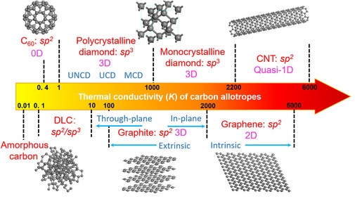
Note that graphite, graphene, and CNT structures are similar chemically – experimental materials analysis with graphite is easier, and can ultimately be extended to CNT processing.
At the recent IEDM conference, TSMC provided an intriguing update on their progress with CNT device fabrication. [1] This article summarizes the highlights of that presentation.
CNT devices offer some compelling features:
- very high carrier mobility (> 3,000 cm**2/V-sec, “ballistic transport”, with minimal scattering)
- very thin CNT body dimensions (e.g., diameter ~1nm)
- low parasitic capacitance
- excellent thermal conduction
- low temperature (<400C) processing
The last feature is particularly interesting, as it also opens up the potential for integration of silicon-based, high-temperature fabrication with subsequent CNT processing.
Gate Dielectric
A unique process flow was developed to provide the “high K” dielectric equivalent gate oxide for a CNT device, similar to the HKMG processing of current silicon FETs.

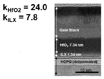
The TEM figure above illustrates the CNT cross-section. Deposition of an initial interface dielectric (Al2O3) is required for compatibility with the unique carbon surface – i.e., suitable nucleation and conformity of this thin layer on carbon are required.
Subsequently, atomic level deposition (ALD) of a high-K HfO2 film is added. (These dielectric experiments on material properties were done with a graphite substrate, as mentioned earlier.)
The minimum thicknesses of these gate dielectric layers is constrained by the requirement for very low gate leakage current – e.g., <1 pA/CNT, for a gate length of 10nm. The test structure fabrication for measuring gate-to-CNT leakage current is illustrated below. (For these electrical measurements, the CNT structure used a quartz substrate.)
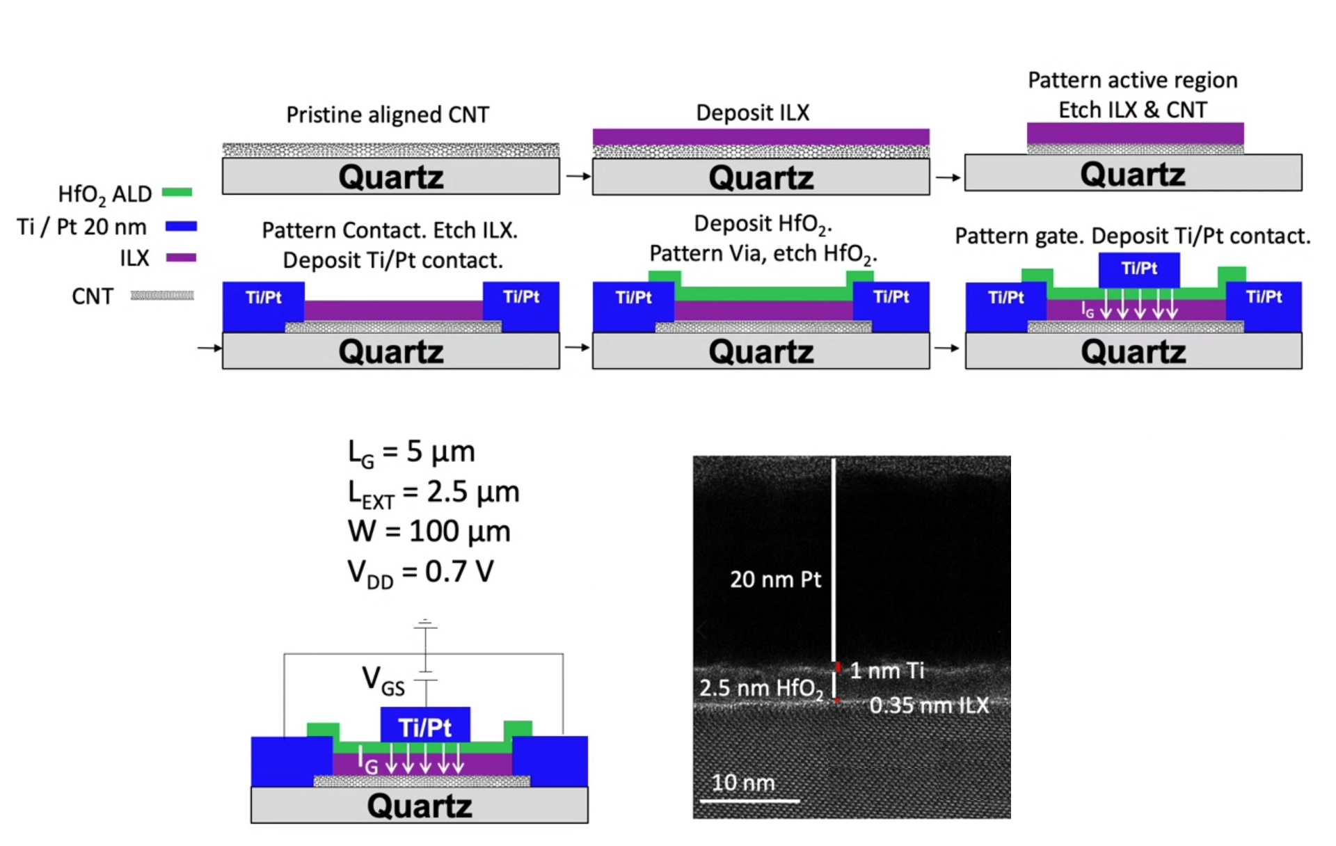
The “optimal” dimensions from the experiments results in t_Al2O3 = 0.35nm and t_HfO2 = 2.5nm. With these extremely thin layers, Cgate_ox is very high, resulting in improved electrostatic control. (Note that these layers are thicker than the CNT diameter, the impact of which will be discussed shortly.)
Gate Orientation
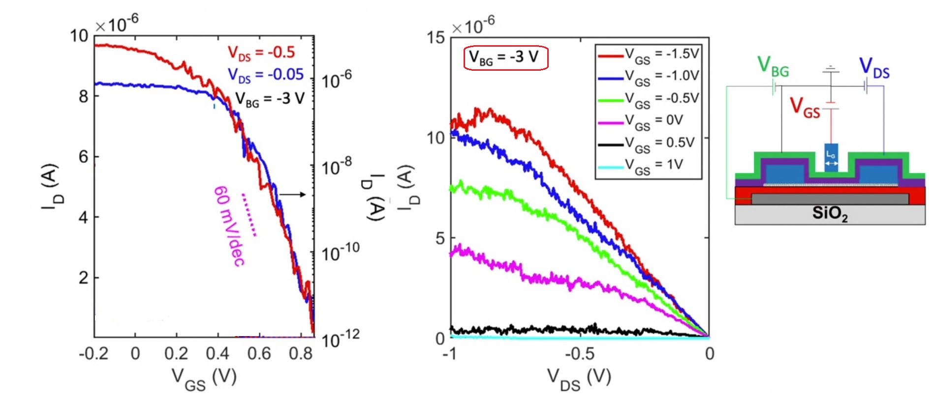
The CNT devices evaluated by TSMC incorporated a unique “top gate plus back gate” topology.
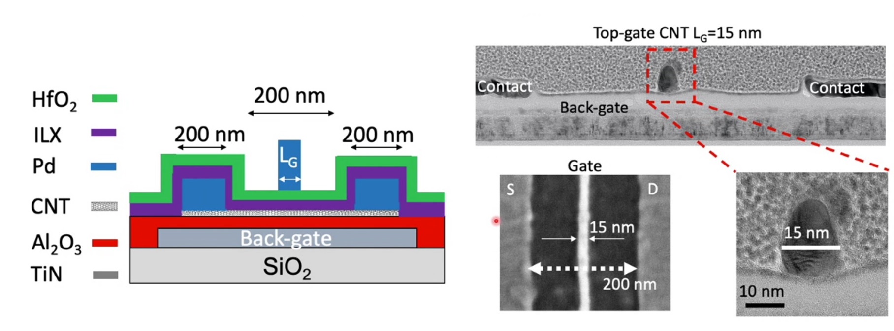
The top gate provides the conventional semiconductor field-effect device input, while the (larger) back gate provides electrostatic control of the carriers in the S/D extension regions, to effectively reduce the parasitic resistances Rs and Rd. Also, the back gate influences the source and drain contact potential between the CNT and Palladium metal, reducing the Schottky diode barrier and associated current behavior at this semiconductor-metal interface.
Device current
The I-V curves (both linear and log Ids for subthreshold slope measurement) for a CNT pFET are depicted below. For this experiment, Lg = 100nm, 200nm S/D spacing, CNT diameter = 1nm, t_Al2O3 = 1.25nm, t_HfO2 = 2.5nm.
For this test vehicle (fabricated on a quartz substrate), a single CNT supports Ids in excess of 10uA. Further improvements would be achieved with thinner dielectrics, approaching the target dimensions mentioned above.
Parallel CNTs in production fabrication will ultimately be used – the pertinent fabrication metric will be “the number of CNTs per micron”. For example, a CNT pitch of 4nm would be quoted as “250 CNTs/um”.
Challenges
There are certainly challenges to address when planning for CNT production (to mention but a few):
- regular/uniform CNT deposition, with exceptionally clean surface for dielectric nucleation
- need to minimize the carrier “trap density” within the gate dielectric stack
- optimum S/D contact potential materials engineering
- device modeling for design
The last challenge above is especially noteworthy, as current compact device models for field-effect transistors will definitely not suffice. The CNT gate oxide topology is drastically different than a planar or FinFET silicon channel. As the gate-to-channel electric field is radial in nature, there is not a simple relation for the “effective gate oxide”, as with a planar device.
Further, the S/D extensions require unique Rs and Rd models. Also, the CNT gate oxide is thicker than the CNT diameter, resulting in considerable fringing fields from the gate to the S/D extensions and to the (small pitch separated) parallel CNTs. Developing suitable compact models for CNT-based designs is an ongoing effort.
Parenthetically, a CNT “surrounding gate” oxide – similar to the gate-all around nanosheet – would be an improvement over the deposited top gate oxide, but difficult to manufacture.
TSMC is clearly investing significant R&D resources, in preparation for the “inevitable” post-silicon device technology introduction. The results on CNT fabrication and electrical characterization demonstrate considerable potential for this device alternative.
-chipguy
References
[1] Pitner, G., et al, “Sub-0.5nm Interfacial Dielectric Enables Superior Electrostatics: 65mV/dec Top-Gated Carbon Nanotube FETs at 15nm Gate Length”, IEDM 2020.
Share this post via:


Comments
There are no comments yet.
You must register or log in to view/post comments.