You are currently viewing SemiWiki as a guest which gives you limited access to the site. To view blog comments and experience other SemiWiki features you must be a registered member. Registration is fast, simple, and absolutely free so please,
join our community today!
WP_Term Object
(
    [term_id] => 157
    [name] => EDA
    [slug] => eda
    [term_group] => 0
    [term_taxonomy_id] => 157
    [taxonomy] => category
    [description] => Electronic Design Automation
    [parent] => 0
    [count] => 4514
    [filter] => raw
    [cat_ID] => 157
    [category_count] => 4514
    [category_description] => Electronic Design Automation
    [cat_name] => EDA
    [category_nicename] => eda
    [category_parent] => 0
    [is_post] =>
)
SemiWiki broke the story yesterday about the Cadence legal action against Berkeley Design Automation and today I spent time with customers of both companies in Silicon Valley getting reactions. That is the advantage of working in Silicon Valley for almost 30 years, if you don’t know the right people, you certainly know the people… Read More
I talked to Michael Buehler-Garcia about the changes Mentor is making to U2U, their user conference. It is in San Jose on April 25th at the DoubleTree.
Firstly, there are 3 great keynotes, two of whom I’ve seen speak before and can unreservedly recommend. Unfortunately I’m traveling that week and won’t be able… Read More
Cadence has brought a suit against Berkeley Design Automation for, as far as I can see, integrating their AFS circuit simulator with the Virtuoso Analog Design Environment (ADE) without using the (licensed) Oasis product. Since BDA is (actually was) a member of the Cadence Connections program, they have to abide by the contract… Read More
As we have moved towards lower process nodes to improve performance of ICs with higher density and functionality, many manufacturing effects have appeared which can render ICs useless, even though the layout design could be correct as per traditional design rules. What is more worrisome is the variability of these effects which… Read More
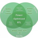
RTL Power Optimizationby Paul McLellan on 04-09-2013 at 10:23 amCategories: EDA
More so than most aspects of design, power reduction suffers from a paradox that early in the design cycle when the gains are the largest, the accuracy of power estimation is the lowest, and then late in the design cycle, when everything is known pretty much exactly it is too late to make anything other than trivial optimizations. … Read More
At DAC in 2012 I visited a few dozen EDA companies and blogged 32 articles, however I didn’t get to see what Apache Design (now a subsidiary of ANSYS) had to say. I did have 20 minutes today to watch their latest video on SoC Power Integrity Challenges and decided to share what I learned. If you want to watch the video at Tech Online,… Read More
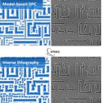
Cutting the Key to 14nm Lithographyby Beth Martin on 04-08-2013 at 2:30 pmCategories: EDA, Siemens EDA
It appears that immersion lithography is now the plan of record for manufacturing ICs at 14nm. How is it possible to use 193nm wavelength light at 14nm? How can we provide the process window to pattern the such tight pitches? The secret lies in computational lithography. For 20nm, the two key innovations in computational lithography… Read More
… is now 8 years old, and the money paid for this 10 engineers start-up was considered, at that time, as a “bingo” for Cascade’s funders: “In October 2004, the Company completed the acquisition of Cascade Semiconductor Solutions, Inc. (Cascade) for total upfront consideration of $15.8 million and contingent consideration of … Read More
My background is IC design engineering, so it’s always a delight to talk with another engineer on their chip challenges. Today I spoke by phone with Sucharita Biswas, a Senior Hardware Engineer at Altera involved in IC test debug for FPGA devices.
… Read More
April 25, 2013, San Jose, CA
Click here to register.
Come hear Mentor Graphics CEO, Wally Rhines, 2013 Kaufman Award Winner,Chenming Hu, and Xilinx Senior VP,Victor Peng, at the User2User Conference in San Jose.
KEYNOTES
Organizing by Design
9:00am – 9:50am
Walden C. Rhines | CEO & Chairman | Mentor Graphics
Winning products… Read More


Consolidation and Competition: Who is Winning the $4.5 Billion Interface IP Race?