You are currently viewing SemiWiki as a guest which gives you limited access to the site. To view blog comments and experience other SemiWiki features you must be a registered member. Registration is fast, simple, and absolutely free so please,
join our community today!
WP_Term Object
(
    [term_id] => 157
    [name] => EDA
    [slug] => eda
    [term_group] => 0
    [term_taxonomy_id] => 157
    [taxonomy] => category
    [description] => Electronic Design Automation
    [parent] => 0
    [count] => 4173
    [filter] => raw
    [cat_ID] => 157
    [category_count] => 4173
    [category_description] => Electronic Design Automation
    [cat_name] => EDA
    [category_nicename] => eda
    [category_parent] => 0
    [is_post] =>
)
See how Synopsys’ advanced analog verification solution can dramatically increase your verification productivity with CustomExplorer Ultra, along with CustomSim and CustomSim-VCS. CustomExplorer Ultra is a comprehensive simulation and debug environment for analog and mixed-signal design verification.
Web … Read More
First, I must say that I’m biased. I like Cheerleaders, they are lots of fun, I even married one. Second, I’m not a fan of Peggy Aycinena. She has been on her EDA feminist rant for years now and I have been targeted multiple times. My solution has been to ignore her and any publication that supports her but this time she has gone too far.… Read More
If you are involved in testing memory or logic of ARM-based designs, you’ll want to attend this free seminar on July 17, 2012 in Santa Clara. Mentor Graphics and ARM have a long standing partnership, and have optimized the Mentor test products (a.k.a Tessent) for the ARM processors and memory IP.
The lunch seminar runs from 10:30-1:00… Read More
Next week it is Semicon West in the Moscone Center from Tuesday to Thursday, July 10-12th. Cadence will be on a panel session during a session entitled The 2.5D and 3D packaging landscape for 2015 and beyond. This starts with 3 short keynotes:
- 1.10pm to 1.25pm: Dr John Xie of Altera on Interposer integration through chip on wafer on
…
Read More
In my circuit design past I did DRAM work at Intel, so I was interested in learning more about Novocell Semiconductor and their design of One Time Programmable (OTP) IP. Walter Novosell is the President/CTO of Novocell and talked with me by phone on Thursday.… Read More
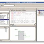
At DAC in June I didn’t get a chance to visit ClioSoft for a product update so instead I read their white paper this week, “The Power of Visual Diff for Schematics & Layouts“. My background is transistor-level IC design so anything with schematics is familiar and interesting.
The Challenge
Hand-crafted … Read More
SEMICON West is coming up this July 10-12 at the Moscone Center in San Francisco. It covers a broad swath of the microelectronics supply chain, but I was particularly interested in the test sessions. Here are two that I recommend.
“The Value of Test for Semiconductor Yield Learning” on Tuesday, July 10, at 1:30p. The… Read More
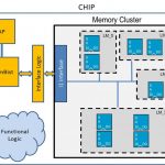
If we look at SoC design evolution, we have certainly successfully passed several steps: from transistor by transistor IC design using Calma up to design methodology based on the integration of 500K + gates IP like PCIe gen-3 Controller, one out of several dozens of IP integrated in today’ SoC for Set-Top-Box or Wireless Application… Read More
For those of you who didn’t get to DAC you can catch up on low power issues with Apache’s series of low-power webinars taking place late in July. All webinars are at 11am Pacific Time. Full details and registration on the Apache website here.… Read More
Synopsys is the dominant player in the commercial EDA and semiconductor IP markets so it is always interesting to hear what John Koeter, Vice President of Marketing for IP, Services and System Level Solutions, has to say. John presented “The Role of IP in a Changing Landscape” at the SemiCO IMPACT Conference and I talked to him again… Read More


Flynn Was Right: How a 2003 Warning Foretold Today’s Architectural Pivot