You are currently viewing SemiWiki as a guest which gives you limited access to the site. To view blog comments and experience other SemiWiki features you must be a registered member. Registration is fast, simple, and absolutely free so please,
join our community today!
WP_Term Object
(
    [term_id] => 157
    [name] => EDA
    [slug] => eda
    [term_group] => 0
    [term_taxonomy_id] => 157
    [taxonomy] => category
    [description] => Electronic Design Automation
    [parent] => 0
    [count] => 4617
    [filter] => raw
    [cat_ID] => 157
    [category_count] => 4617
    [category_description] => Electronic Design Automation
    [cat_name] => EDA
    [category_nicename] => eda
    [category_parent] => 0
    [is_post] =>
)
The number one EDA+IP vendor in our industry today is Synopsys, and their eloquent leader is Aart de Geus, so I expect that the Monday interview at #53DAC on June 6th will be well attended and worthwhile to witness in the DAC Pavilion, start time is 11:30AM, so arrive early to get a seat. One of Aart’s coined words is Technomics,… Read More
For bloggers like myself spending four days at #53DAC is almost a non-stop blur of activity, visiting EDA vendors, IP providers and foundries to learn about what’s happening in our semiconductor industry. Cadence is both an EDA vendor and IP provider, so DAC is a great showcase for them to tell us what’s new in 2016 and… Read More
I live in Tualatin, Oregon just a few miles away from the corporate headquarters of the #3 EDA company in the world, Mentor Graphics. Since DAC is fast approaching, I thought it would be useful to give you a quick overview of what Mentor is going to be talking about in Austin, Texas during June 5-9. … Read More
When I hear the company name of ANSYS the first EDA tool category that comes to mind is power noise sign-off. Going to DAC is a great way to find out what’s new with EDA, IP and foundries. There are three places that you can find ANSYS at DAC this year:… Read More
The design community is always hungry for high-performance, low-power, and low-cost devices. There is emergence of FinFET and FDSOI technologies at ultra-low process nodes to provide high-performance and low-power requirements at lower die-size. However, these advanced process nodes are prone to new sources of variation.… Read More
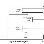
Power protection chips are widely used these days to protect sensitive circuitry from over-voltage and over-current stress. However, these workhorse chips are often subjected to extraordinary thermal stress themselves and need to be protected from burning up – literally.
Power protection chips work like electronic fuses,… Read More
In the pages of SemiWiki, we are usually talking about what to do with billions of really small transistors – for a change of pace today, we’ll discuss what to do with a few really big ones. Mentor Graphics has just announced their latest MicReD platform for thermal testing of IGBTs, experiencing a resurgence (pun intended) thanks… Read More
Design starts are critical to the growth of the semiconductor industry so enabling them is a common theme on SemiWiki. One thing we have not covered in detail is multi-project wafer services (MPW) which is the equivalent of ride sharing through the initial mask and wafer process. Larger semiconductor companies already do this … Read More
A common SoC design methodology in current use starts with preparation of the physical floorplan — e.g., block/pin placement, global clock domain and bus signal planning, developing the global/local power distribution (and dynamic power domain management techniques). Decoupling capacitor estimated densities and… Read More
Rebooting EDAby Bernard Murphy on 05-23-2016 at 7:00 amCategories: Ansys, Inc., EDA
In the 35 years since commercial EDA went mainstream a lot of advances have been made but the fundamental architecture and even the philosophy of tooling have really not advanced at all. Tools are designed around individual tasks – analysis and optimization within a specific domain – under the assumption that variability within… Read More











The silent killer of analog reliability: Why SPICE misses floating net