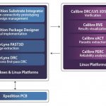
There is an emerging set of advanced packaging technologies that enables unique product designs, with the capability to integrate multiple die, from potentially heterogeneous technologies. These “system-in-package” (SiP) offerings provide architects with the opportunity to optimize product performance, power, cost,… Read More
Author: Tom Dillinger
Embedded FPGA IP update — 2nd generation architecture, TSMC 16FFC, and a growing customer base
Regular Semiwiki readers are aware that embedded FPGA (eFPGA) IP development is a rapidly growing (and evolving) technical area. The applications for customizable and upgradeable logic in the field are many and diverse — as a result, improved performance, greater configurable logic capacity/density, and comprehensive… Read More
3D Product Design Collaboration in MCAD and ECAD Platforms
Consumer electronics demand aggressive mechanical enclosure design — product volume, weight, shape, and connector access are all critical design optimization criteria. Mechanical CAD (MCAD) software platforms are used by product engineers to develop the enclosure definition — the integration of the PCB design… Read More
The 4C’s of PCB Design
The diamond jewelry industry encourages customers to focus on the 4C’s — cut, clarity, color, and carats. At the recent PCB Forum conducted by Mentor (a Siemens business) in Santa Clara, I learned that current system design flows also require an emphasis on the 4C’s — collaboration, concurrency, consistency… Read More
TSMC Design Enablement Update
A couple of recent semiwiki articles reviewed highlights of the annual TSMC Technical Symposium recently held in Santa Clara (links here, here, and here). One of the captivating sessions at every symposium is the status of the Design Enablement for emerging technologies, presented at this year’s event by Suk Lee, Senior… Read More
Top 10 Updates from the TSMC Technology Symposium, Part II
An earlier article described some of the technical and business highlights from the recent TSMC Symposium in Santa Clara (link). This article continues that discussion, with the top five updates.… Read More
Top 10 Updates from the TSMC Technology Symposium, Part I
Last week, TSMC held their 23rd annual technical symposium in Santa Clara. In the Fall, TSMC conducts the OIP updates from EDA/IP partners and customers. The theme of the Spring symposium is solely on TSMC’s technology development status and the future roadmap. Indirectly, the presentations also provide insight into … Read More
What’s better than silicon-proven IP? Lab bench-proven!
The SoC industry depends upon the availability of validated IP. SoC designs require a huge investment, and assume the external IP that is licensed from outside parties satisfies all functional and electrical specifications. To support that requirement, IP providers typically pursue a strategy to demonstrate their designs… Read More
PowerTree — a data repository and simulation platform for PCB power distribution networks
The difficulty of managing the power domains on a complex SoC led to the development of a power format file description, to serve as the repository for data needed for functional and electrical analysis (e.g., CPF, UPF). Yet, what about complex printed circuit boards? How can the power domain information be effectively represented… Read More
Power and Performance Optimization for Embedded FPGA’s
Last month, I made a “no-brainer” forecast that 2017 would be the year in which embedded FPGA (eFPGA) IP would emerge as a key differentiator for new SoC designs (link to the earlier article here).
The fusion of several technical and market factors are motivating design teams to incorporate programmable logic functionality… Read More


Intel, Musk, and the Tweet That Launched a 1000 Ships on a Becalmed Sea