I first visited STat their Agrate, Italy site where Flash memory development is done. At DACthis year Antonio Bogani talked about how ST designs with LDE while using EDA tools and a PDK (Process Design Kit) from Cadence. They recorded the 17 minute presentation, and you can view it herewithout having to register. Antonio’s group provides the technology R&D for Smart Power products that is used in markets like:
- Digital consumer products
- Microcontrollers
- MEMS & Sensors
- Automotive products
- Smart Power products (digital, analog and power modules combined) using Bipolar, CMOS + DMOS(BCD)
Process technology ranges from 90nm to .32um nodes which are well suited for high-voltage applications. Custom IC design at the transistor-level for BCD designs must take into account LDE like:
- Shallow Trench Isolation (STI)
- Well Proximity Effects (WPE)
Related: Samsung 14 nm FinFET Design with Cadence Tools
Process rules are difficult to manage because of:
- Halation and other non-simple backend rules
- Rounded corners of polygons to smooth high-voltage electrical fields
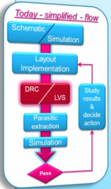
The old design approach was quite sequential and had a long feedback loop requiring slow iterations during design:
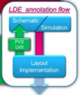
A new design approach does LDE analysis of STI and WPE while doing layout, then annotates the effects into the schematics, ready for simulation:
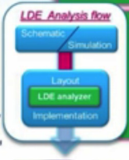
You can also do an LDE analysis flow on incomplete layout inside the Virtuoso XL layout tool, where Spectre is used to simulate and then display LDE deviations on device parameters like: Vth, Ids. This provides you with verification that constraints were met in the presence of LDE on your critical devices.
While you are drawing an IC layout you can turn on real-time DRC verification, taking less than a second or so and providing visual feedback as violation markers. Another way to verify is DRC on demand, typically on the visible area, taking 15 seconds or less.
Related: A Deeper Insight into Quantus QRC Extraction Solution
By using the Cadence PDK with MODGENs or partial layout you can get to a simulation netlist even with just a prototype placement, then simulate the LDE effects using the Analog Design Environment – ADE XL for short. Layout parameters are quickly added to the schematic.
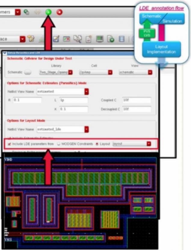
By having such quick feedback you are receiving early detection of LDE variability hotspots and making layout fixes much easier than waiting for a final layout. The DFM PDK flow is shown below:
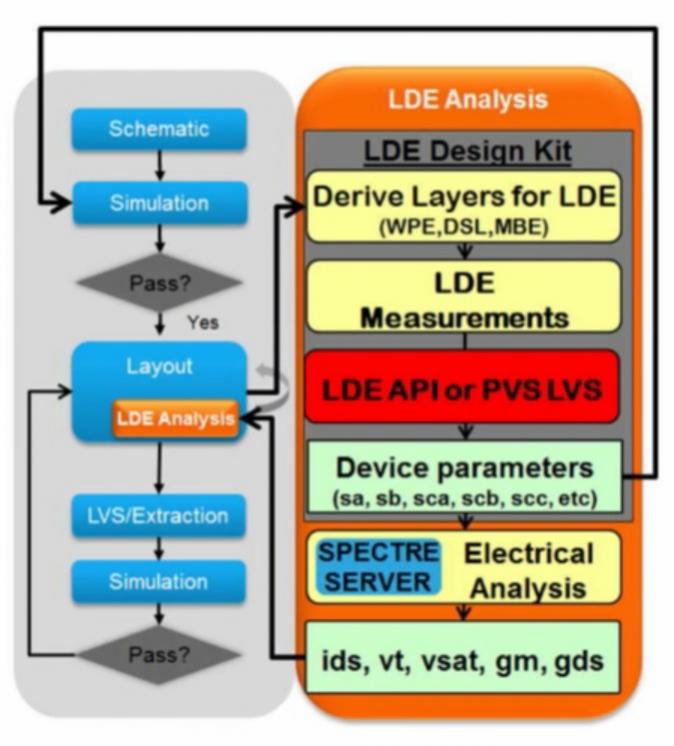
Groups at ST are using this type of flow on their bcd8 and bcd8 families PDK. The benefits of using a Cadence in-design flow are to accelerate IC development on Smart Power projects in process technologies with LDE.
Related: 10 nm, the View from IBM
Share this post via:


Comments
0 Replies to “How ST Designs with Layout Dependent Effects (LDE)”
You must register or log in to view/post comments.