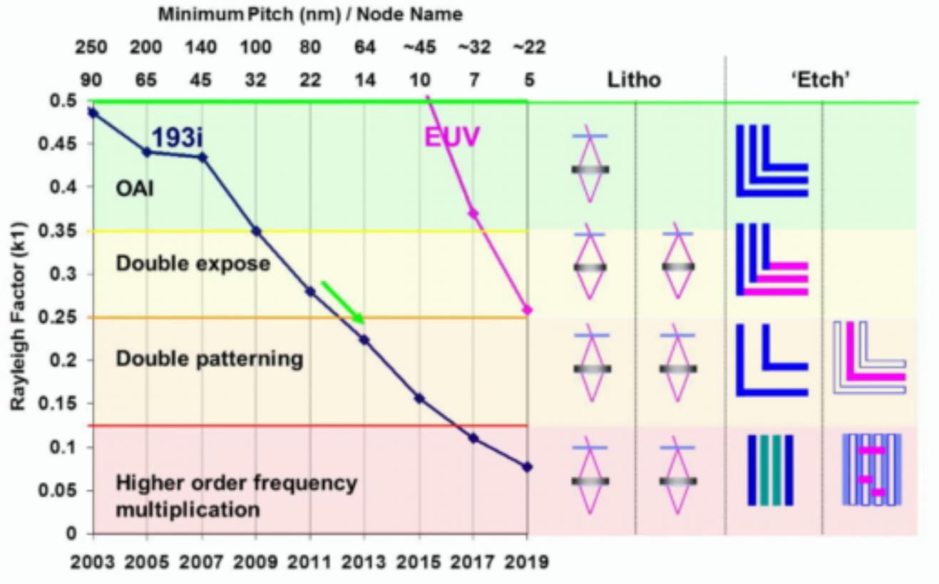
 On the Cadence booth at DAC, Lars Liebmann of IBM presented on the challenges of 10nm. As he put it, how the lithography folks are keeping things very interesting for the EDA tool development engineers. Although 14nm/16nm hasn’t yet ramped into HVM, the advanced work for tools and IP has all moved to 10nm. Although Lars gave the presentation, it is also credited to Vassilios Gerousis, Mike Zhang and Paul Gutwin of Cadence, Geng Han of IBM and Brian Cline of ARM. I talked to Lars this week and got a copy of the presentation but there is a video of the whole thing on the Cadence website. See below for a link.
I’m going to take it as given that you know all about double patterning, and I’m going to take it as given that EUV is not going to be available at 10nm. We have to live with 193nm light.
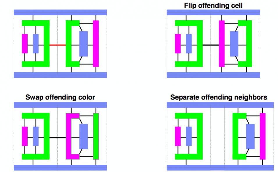
At 10nm, the first change is that even though we are still in the double patterning resolution window, we need to add a third color to resolve odd cycles, carefully optimized design rules are not enough to prevent cell to cell color interactions. When two cells are placed next to each other that conflict, there are three approaches to fixing it in the placer: flip the offending cell so it no longer offends, spread the offending cells further apart, or swap the offending color (since the power lines are one color that we can swap from cell to cell, even with 3 colors there is actually only a single choice of what colors to swap).
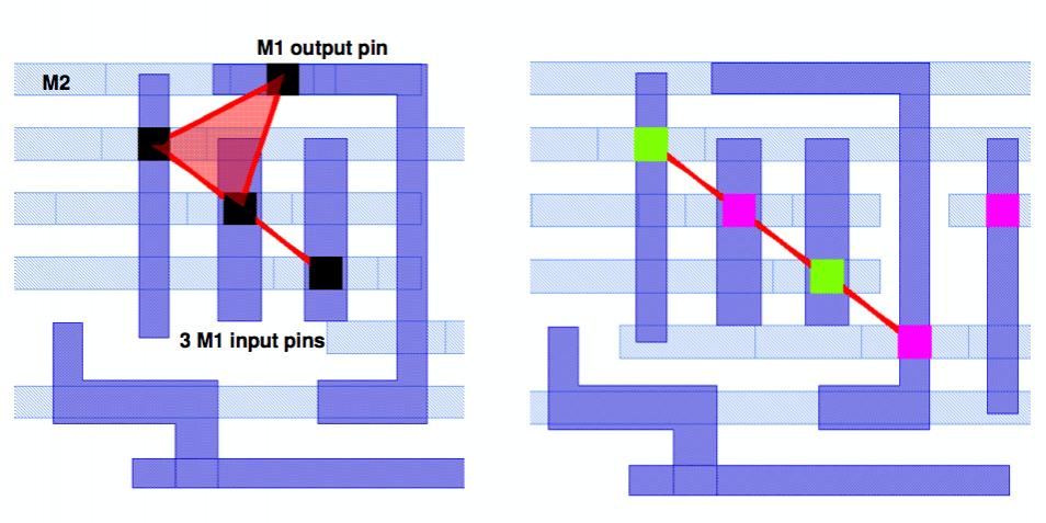
Vias are another problem. Even at 14nm we can’t put two vias next to each other in the obvious way, they are too close. The nearest alternatives are diagonally adjacent. But at 10nm the area of interaction is so large that not just neighboring vias but the two vias over need to be colored appropriately. This cannot be done after the routing has been completed, since it would often turn out to be impossible. Instead explicit odd cycle via prevention is required in the router.
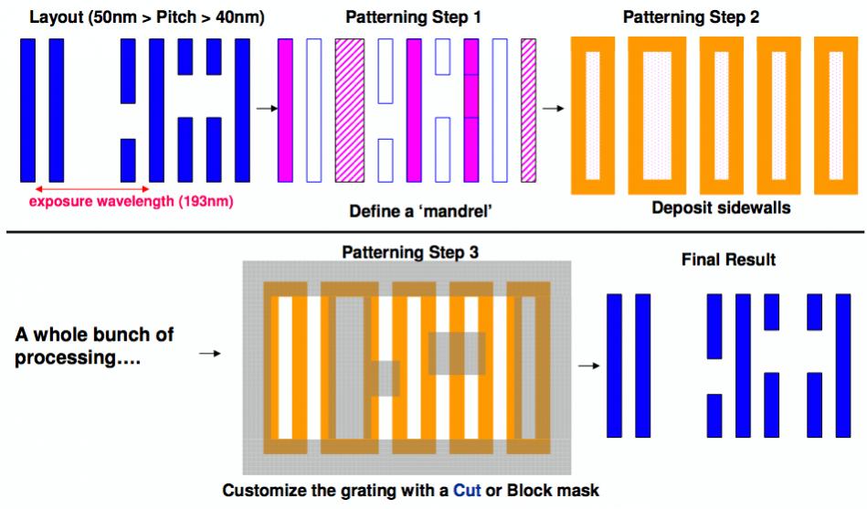
The type of double patterning used at 14nm is known as LELE for litho-etch-litho-etch. But there are resolution limits to this limited by overlay and also dielectric breakdown. So for 10nm we will need what is called either SIT (sidewall image transfer) or SADP (self-aligned double patterning). In this a mandrel is created, sidewalls are created on the edge of the mandrel, and then a cut/block mask is used to trim the design and remove unwanted parts. But arbitrary layout can lead to errors (non-manufacturability) on the block mask. A whole new lot of line end stagger rules come into play. The block mask patterning becomes the resolution limiter.
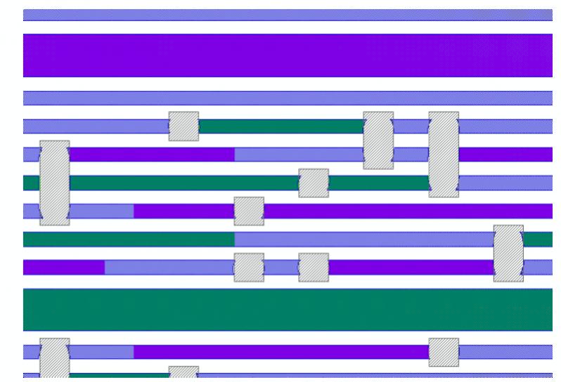
The solution is to go to a sea of wires with a highly constrained cut mask. This means lengthening many wires (which will affect performance), creating dummy floating wires and worrying about line-end stagger control.
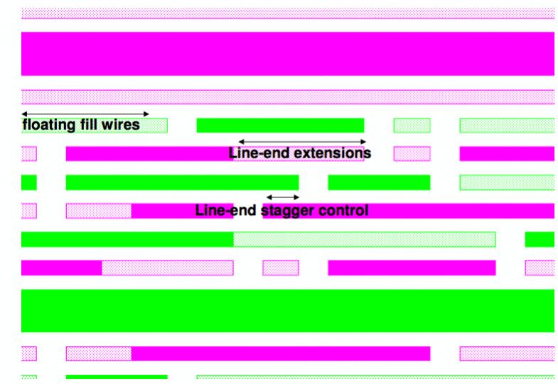
All of this has been implemented in Cadence’s Encounter and with a compliant ARM 9-track standard cell library.
The video of Lars’s presentation is here. It is the presentation at 11am on Tuesday.
More articles by Paul McLellan…


Comments
0 Replies to “10nm, the View from IBM”
You must register or log in to view/post comments.