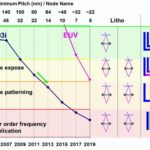
On the Cadence booth at DAC, Lars Liebmann of IBM presented on the challenges of 10nm. As he put it, how the lithography folks are keeping things very interesting for the EDA tool development engineers. Although 14nm/16nm hasn’t yet ramped into HVM, the advanced work for tools and IP has all moved to 10nm. Although Lars gave… Read More
Tag: triple patterning
Imec’s Process Secret Decoder Ring
To wrap up Semicon West, let’s go back to Monday and the imec presentations. In fact, An Steegen’s presentation titled The Semiconductor Roadmap. She covered a lot of ground, but some of her slides contain a wealth of information. Let’s look at the options for 10nm, 7nm and a little 5nm, what imec call N10, N7 and… Read More
Triple Patterning
As you can’t have failed to notice by now, 28nm is the last process node that does not require double patterning. At 20nm and below, at least some layers require double patterning. The tightest spacing is typically not the transistors but the local interconnect and, sometimes, metal 1.
In the litho world they call double patterning… Read More
The Rosetta Stone of Lithography
At major EDA events, CEDA (the IEEE council on EDA, I guess you already know what that bit stands for) hosts a lunch and presentation for attendees and others. This week was ICCAD and the speaker was Lars Liebmann of IBM on The Escalating Design Impact of Resolution-Challenged Lithography. Lars decided to give us a whirlwind tour … Read More


