





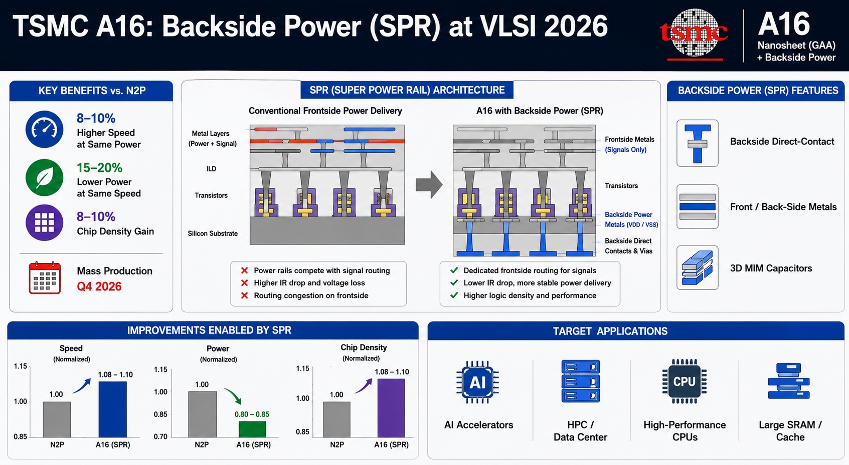
TSMC’s A16 technology, presented as Paper T1.5 at the June 2026 IEEE/JSAP VLSI Symposium, marks the company’s first angstrom-class CMOS platform combining enhanced nanosheet gate-all-around transistors with backside power delivery. The key integration feature is Super Power Rail, or SPR, which TSMC describes as a backside direct-contact power delivery scheme targeted at AI and high-performance-computing designs with dense power grids and complex signal routing. Compared with N2P, the VLSI abstract reports 8–10% higher speed at the same power, or 15–20% lower power at the same speed, plus 8–10% chip-density gain, with mass production slated for Q4 2026.
The technical motivation is straightforward: at advanced nodes, frontside metal stacks are increasingly congested. Conventional power rails compete with signal interconnect for routing tracks, and resistive voltage loss, or IR drop, becomes harder to control as supply voltages fall and current density rises. By moving the primary power distribution network to the wafer backside, A16 separates power delivery from frontside signal routing. This releases frontside resources for timing-critical interconnect while creating a lower-resistance path for VDD/VSS delivery. TSMC’s public A16 page states that SPR improves logic density and performance by dedicating frontside routing to signals and significantly reducing IR drop.
A notable part of TSMC’s approach is the backside direct contact architecture. Rather than only placing large backside power metals underneath the device layer, SPR connects backside power more directly into the transistor source/drain region through backside vias and contacts. The VLSI technical tipsheet describes A16-SPR as using backside direct-contact power delivery, front/back-side metals, and 3D MIM capacitors, indicating that the power-delivery system is not merely a routing rearrangement but a full process-integration module.
This matters because backside power can create tradeoffs in cell height, device width, standard-cell architecture, and design-technology co-optimization. TSMC emphasizes that its backside contact scheme preserves N2P gate density and NanoFlex design flexibility, meaning designers can still tune cell layouts for performance, power, and area rather than being locked into a single restrictive cell template. The VLSI session abstract specifically says SPR preserves N2P gate density and NanoFlex DTCO benefits, which is important for real product implementation rather than only test-chip demonstration.
For AI and HPC chips, A16’s benefit is especially relevant. Large accelerators have massive simultaneous switching currents, long global routes, high SRAM/cache content, and strict timing closure requirements. Reducing IR drop improves effective transistor drive because less voltage is lost before reaching active devices. Freeing frontside routing also helps high-utilization logic blocks where congestion can otherwise force longer wires, more buffers, or larger cells. In practice, SPR should improve both electrical efficiency and physical-design closure, particularly for compute tiles, CPU cores, and accelerator fabrics.
Bottom line: A16 represents more than a node shrink. It is a structural change in how power and signals are partitioned across the chip stack. The result is a process positioned between classic two-dimensional scaling and future three-dimensional logic integration: nanosheet devices provide gate control, while backside power attacks interconnect and power-delivery bottlenecks. At VLSI 2026, TSMC’s message was that A16 is already qualified as a platform technology and moving toward production, making backside power delivery a near-term manufacturing feature rather than a distant research concept.
Also Read:
Why Huawei Says It Will Match TSMC’s Most Advanced Chips by 2031
TSMC Expands Use of NVIDIA AI Technologies Across Chip Production Operations




Comments
There are no comments yet.
You must register or log in to view/post comments.