






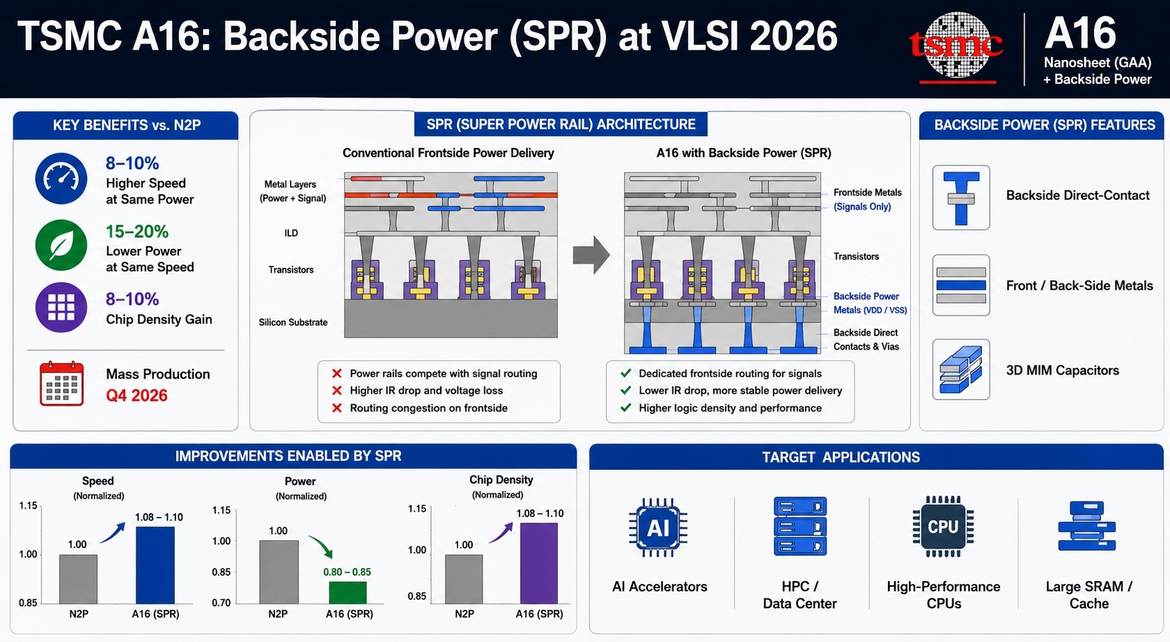
TSMC Super Power Rail (SPR) is TSMC’s implementation of backside power delivery for advanced logic semiconductor nodes. It is publicly associated with TSMC’s A16 process technology, an angstrom-class node that combines nanosheet transistors with a new power-delivery architecture intended to improve performance, routing density, and power efficiency. TSMC describes A16 as integrating nanosheet devices with “Super Power Rail” solutions to improve logic density and performance.
In conventional integrated-circuit layouts, both signal interconnects and power-delivery networks are routed mainly on the front side of the wafer, above the transistor layer. As transistors shrink and current demand rises, this shared routing space becomes increasingly congested. Power rails consume metal resources that could otherwise be used for signal routing, while long and narrow power paths contribute to resistive voltage loss, commonly known as IR drop. These effects are especially important in high-performance computing, artificial intelligence accelerators, and dense system-on-chip designs, where local current density can be very high.
SPR addresses this problem by moving a significant portion of the power-delivery network to the backside of the wafer. In a backside power-delivery network, power is delivered from below the transistor layer, while the front-side interconnect stack is used more efficiently for signal wiring. This separation can reduce routing congestion, lower resistance in the power grid, and improve voltage stability at the transistor level. Industry descriptions of TSMC’s SPR indicate that it connects the backside power network directly to transistor source/drain regions through specialized backside contacts, rather than relying only on more indirect buried or front-side rail structures.
The principal technical goals of SPR are improved power integrity, higher usable cell density, and better performance-per-watt. Reduced IR drop allows circuits to operate closer to their intended supply voltage under load, which can improve frequency headroom or allow lower operating voltage for the same target speed. By removing or reducing front-side power-rail competition with signal wires, SPR can also increase standard-cell routing efficiency and make dense logic blocks easier to implement. This is important because modern process scaling is no longer driven only by transistor gate length; interconnect resistance, capacitance, routing congestion, and power delivery increasingly determine practical chip performance.
SPR is part of a broader industry transition toward backside power delivery. Intel markets a related approach as PowerVia, while other foundries and research groups have explored buried power rails, backside vias, and hybrid power-distribution schemes. TSMC’s claimed distinction is the specific integration of SPR with its nanosheet transistor platform and A16 design rules. According to Reuters, TSMC announced A16 in 2024 and said it would begin production in the second half of 2026, with backside power delivery positioned as useful for AI chips. Public roadmap reporting in 2026 suggested that A16 timing may have shifted toward 2027, illustrating that exact node ramp dates can change as process integration and customer schedules mature.
Manufacturing SPR is technically challenging. Backside power delivery typically requires wafer thinning, backside alignment, contact formation from the wafer backside, and careful integration with front-side transistor and interconnect processes. These steps must preserve transistor performance, yield, thermal behavior, and mechanical reliability. Thermal design is also a concern because backside structures can alter heat flow paths, particularly in 2.5D and 3D packages where chiplets and stacked components already complicate cooling.
SPR is most relevant to high-end processors, AI accelerators, GPUs, networking chips, and other designs where dense logic, high current delivery, and performance-per-watt are critical. It is less likely to be an immediate requirement for cost-sensitive or analog-heavy products, where mature nodes may offer better economics. In TSMC’s technology roadmap, SPR represents a scaling booster: a structural innovation intended to extend logic scaling beyond what can be achieved by transistor improvements alone.
Share this post via:







CEO Interview with Charlie Cheng of CEO of TeRAM