webinar IPXACT banner

Conquering the Next IoT Challenges with FPGA-Based Prototyping

Conquering the Next IoT Challenges with FPGA-Based Prototyping
by Daniel Nenni on 07-12-2015 at 12:00 pm

The need for ever-connected devices is skyrocketing. As I fiddle with my myriad of electronic devices that seem to power my life, I usually end up wishing that all of them could be interconnected and controlled through the Internet. The truth is, only a handful of my devices are able to fulfill that wish, but the need is there and developers are increasingly recognizing that we are moving to a connected life. The pressure to create such a connected universe is so immense that designers need a faster, more reliable way to fulfill our insatiable need. Every connected appliance requires software to run it and with the growing number of these gadgets, software development needs must be met to power them. To add to the pressure mix, the competition in this connected space is immense. In other words, if you’re not one of the first to market, your design could be destined for failure.

One way to meet these challenges and alleviate time-to-market apprehension is for designers to adopt FPGA-based prototyping. This proven technique allows designers to explore their designs earlier and faster and thus proceed more quickly with hardware optimization. More to the point, designers can move into software development and software refinement much sooner and conduct the appropriate number of compatibility tests. During software development, testing is critical to make sure the software performs as expected. An error in how the software interoperates with the hardware can be disastrous therefore designers generally execute a large number of tests to achieve the desired interoperability. Without FPGA prototyping, the time it takes to complete the vast number of tests could spell disaster for meeting the precious time-to-market window. With FPGA prototyping, not only can testing be done earlier, more tests can be conducted to achieve optimal results.

In addition, it has to be said that ARM and Xilinx have been at the forefront of enabling today’s embedded designs. It is critical that prototyping technology keep pace with the advancements from ARM and Xilinx.

S2C’s AXI-4 Prototype Ready™ Quick Start Kit based on the Xilinx Zynq® device is part of S2C’s expansive library of Prototype Ready IP and is uniquely suited to next-generation designs including the burgeoning Internet of Things (IoT).

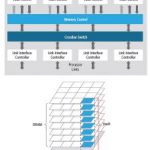
The Quick Start Kit adapts a Xilinx Zynq ZC702 Evaluation Board to an S2C Prodigy Logic Module. The evaluation board supplies a Zynq device containing an ARM dual-core Cortex-A9 CPU and a programmable logic capacity of 1.3M gates. The Quick Start Kit expands this capacity by extending the AXI-4 bus onboard the Zynq chip to external FPGAs on the Prodigy Logic Module Prototyping Platform. This allows designers to quickly leverage a production-proven, AXI-connected prototyping platform with a large, scalable logic capacity – all supported by a suite of prototyping tools.

Integrating Xilinx’s Zynq All Programmable SoC device with S2C’s Virtex-based prototyping system provides designers an instant avenue to large-gate count prototypes centered around ARM’s Cortex-A9 processor.

To learn more about how S2C’s FPGA-based prototyping solutions are enabling the next generation of embedded devices and allow you to realize the Genius of Your Design, visit http://www.s2cinc.com.


Surprisingly Phablets Bucking the Trend

Surprisingly Phablets Bucking the Trend
by Pawan Fangaria on 07-12-2015 at 7:00 am

Amid a fiercely competitive market for computing devices, smartphones, tablets, and so on, a number of devices were created in this decade to invade into each other’s functionalities to either eat away other’s market share or retain their own. The key contenders were smartphones, Phablets, tablets and mini notebooks, whereas the losers were laptops. The smartphones which were earlier shrinking in their sizes started increasing their screen sizes, reincarnating themselves into a new category called ‘Phablets’.

Among so many variants, it was natural for the consumers to get confused choosing between them. Phablet being an in-between device between a phone and a tablet didn’t pick up initially. However, the credit goes to Applewho last year introduced its iPhone 6 Plus with 5.5 inches display that enticed the consumers towards Phablets. It’s then the consumer realized that s/he can manage with just one device which can work as a smartphone as well as a tablet or a mini-laptop, without requiring a separate bag to carry the device. It’s natural the consumer wants maximum functionality in a device along with the convenience to easily handle and operate it anywhere, anytime. The so called Phablets are large display smartphones which are handheld and have several applications including internet web browsing, e-mails, business apps, video gaming and streaming (TV program, movie, other), GPS navigation, camera, and so on.

It’s surprising to see Phablets gaining significant momentum sometime in last year and continuing the trend to surpass the tablet sales this year, and the trend is expected to continue for a few more years. Here is a shipment graph from IC Insights.

In 2014, the large screen smartphones (i.e. Phablets with display sizes of 5 inches or more) unit shipment was at 152 million. In 2015, such smartphone or Phablet shipment is expected to reach 252 million, a whopping 66% increase. According to the IC Insights report, this momentum for Phablets is expected to continue until 2018 at a CAGR of 40%. It’s interesting to know that Apple alone shipped 61.2 million iPhone 6 Plus handsets in the first quarter of this year.

The tablet unit sale in 2015 is forecast to increase by just 2% to reach 238 million units, i.e. much lower compared to Phablets. For a full 2014-2018 period, the tablet CAGR is expected to remain at 3%. The mini tablets in the range of 7” to 9” displays are losing their popularity.

The Phablet share in the total smartphone sales is expected to continuously increase from 17% in 2015 to 21% in 2016 and 30% in 2018. The total smartphone sale is expected to reach 2 billion by 2018.

Shall we see more varieties of larger screen smartphones in the upcoming market? We already have some and more would be coming. Can size only sell?

The IC Insights report is HERE for reference.

Pawan Kumar Fangaria
Founder & President at www.fangarias.com


Who Needs to Lead at the 14, 10 and 7nm nodes

Who Needs to Lead at the 14, 10 and 7nm nodes
by Scotten Jones on 07-11-2015 at 12:00 pm

IBM recently disclosed a working 7nm test chip generating a lot of excitement in the semiconductor industry and also in the mainstream media. In this article I wanted to explore the 14nm, 10nm and 7nm nodes, the status of the key competitors at each node and what it may mean for the companies.

Continue reading “Who Needs to Lead at the 14, 10 and 7nm nodes”


Which High B/W Memory to Select after DDR4?

Which High B/W Memory to Select after DDR4?
by Eric Esteve on 07-11-2015 at 6:00 am

Once upon a time, RAM technology was the driver of the semiconductor process. DRAM products were the first to be designed on a newest technology node and DRAM was used as a process driver. It was 30 years ago and the most aggressive process nodes were ranging between 1um and 1.5 um (1 500 nm!). Then in the 1990 the Synchronous Dynamic Random Access Memory (SDRAM) has been introduced, and the Double Data Rate (DDR) specified in June 2000: the DDR SDRAM was born, and our PC, Laptop or smartphone are still running using this DDR architecture. The DDR4 specification was issued in 2014 (it took 10 years to finalize it) and the industry consensus is that DDR4 will be the last version, don’t ever expect to see DDR5.

Does that mean that DDR4 will disappear? Yes… and no! In fact DDR4 based systems will be developed for a long time, probably up to 2020 and probably later. Why? It’s a pricing related reason! After paying a premium price at introduction, DRAM pricing is declining going to the low range ($ per sq mm of Silicon), so the product is widely used and the price eventually stabilize at a low point. In marketing you call such product a commodity, like beans or nails!

What about new system targeting applications like networking, servers, graphic or the next smartphones? All of these are memory hungry and if you want to offer higher performance than for the previous version (that you do want!), you need to increase the memory interface bandwidth. To do so, you have two options. One is to use a wider data bus (like for example with Wide I/O architecture) the other is to increase the clock speed. Increasing the clock speed for a parallel data bus with a separate clock line (DDRn architecture) inevitably leads to a feasibility limit, say around 4 Gbps for data busses like DDRn. Let’s take a look at two emerging technologies, Hybrid Memory Cube (HMC) and High Bandwidth Memory (HBM) to understand how these architectures could support performance hungry applications.

To write this post I have used resources from the Cadence’s web. The company, being strongly involved in the memory controller and PHY IP market since Denali acquisition, is developing IP to support the post-DDR4 technologies. You can see the related links at the end of this post.

At first we should note that these two protocols, HBM and HMC are based on either 3D or 2.5D technologies. DDR4 is not only the last DDR, it’s also the last protocol based on two dimensions only. To simplify, we can say that 3D is when you package multiple chips (8 memories + 1 logic IC in the above example) using Through Silicon Vias (TSV) to interconnect these chips when 2.5D use a Silicon interposer to interconnect two ICs (IC could be itself a 3D package). This Silicon interposer will be equiped with micro-bumps (50um size) allowing to connect the 2.5D device to a traditional PC board (for example).

Hybrid Memory Cube: 3D + SerDesà360 GB/s
HMC (Figure 4) is being developed by the Hybrid Memory Cube Consortium and has already reach production. The architecture essentially combines SerDes based, high-speed logic process technology with a stack of through-silicon-via (TSV) bonded memory die. According to the Hybrid Memory Cube Consortium, a single HMC can deliver more than 15X the performance of a DDR3 module and consume 70% less energy per bit than DDR3. So, Hybrid Memory Cube is based on ultra-high speed (10, 12.5 or 15 Gbps today, 25 Gbps for the next release) SerDes I/O, the memory chip maker supplying the “cube” also integrating a logic die. Once implemented on a classical board, the memory cube is interfaced with a SoC through several Very High Speed SerDes. The semiconductor industry uses SerDes based interconnects for many years (PCI Express, Ethernet protocols to name a few); special care need to be taken when implementing interconnects on the board, but the feasibility is asserted.

Such architecture providing the highest possible bandwidth (up to 360 GBytes/s today) is attractive for networking applications, but the cost per bit is also the highest, which is not a killing factor for this type of business dedicated applications…

HBM: 2.5D + Wide Data Busà 256 GB/s
HBM (Above Figure) is another emerging memory standard defined by the JEDEC organization. HBM was developed as a revolutionary upgrade for graphics applications. Expected to be in mass production in 2015, the HBM standard applies to stacked DRAM die, and is built using TSV technologies to support bandwidth from 128GB/s to 256GB/s. JEDEC’s HBM task force is now part of the JC-42.3 Subcommittee, which continues to work to define support for up to 8-high TSV stacks of memory on a 1,024-bit wide data interface. In October 2013, the Subcommittee published JESD235: High Bandwidth Memory (HBM) DRAM, which uses wide-interface architecture to achieve high-speed, low-power operation. Please note that HBM is still parallel protocol and that a logic die is inserted between the SoC and the stacked memory dies.

I suggest you to listen to the Whiteboard Wednesday (7/7/2015) where Lou Ternullo is giving a live presentation about specialty memories it last less than 5 minutes and it’s very helpful.

This white paper from cadence: “Five Emerging DRAM Interfaces You Should Know for Your Next Design” will certainly help you deeper your knowledge about these emerging protocols, when “3D Memory Landscape take Shape” specifically addresses the 3D related architectures. The table below is extracted for this paper:

One or several technologies will eventually replace DDR4, but DDR4 will be used doe a long time, especially because it’s the last protocol iteration. The cumulated DDR4 Memory Controller IP sales have weighted more than $100 million in 2014 (source IPnest) and will generate several $100s million during 2015-2020. But IP vendors have to prepare the future and Cadence will have to support some of these emerging technologies.
By Eric Esteve from IPNEST


Tackling Layout Gradient Effects in 16 nm FinFET using Layout Automation

Tackling Layout Gradient Effects in 16 nm FinFET using Layout Automation
by Daniel Payne on 07-10-2015 at 12:00 pm

My first exposure to automating IC layout was back in the 1980’s at Intel where I coded a layout compiler to auto-generate about 6% of a graphics processor chip. The need to use automation for IC layout continues today, and with the advent of FinFET technology there are some new challenges like layout gradient effects that impact yield. I just finished viewing an archived webinar on this topic from experts at TSMC and Cadence, and will summarize what I learned about layout automation.

Captain Liu from TSMC started out and talked about the challenges of FinFET technology for custom IC design, like:

  • Increased complexity in layout design rules
  • Layout pattern effects

    • Layout-dependent effect
    • Density gradient effect
    • Self-heating effect
  • Running circuit simulation without layout effects

The approach engineered at TSMC required close collaboration with Cadence to address these challenges and it uses transistor-level layout generators called ModGens. Here’s the flow starting with schematic capture where the circuit designer sets up constraints like identifying a differential pair of transistors, running pre-layout circuit simulation including LDE effects, then creating layout automatically with a ModGen that understands density checking.

TSMC has created a device array API that reads technology-specific information from the PDK, runs DRC checks, and is aware of all the layout-dependent effects plus density checking. Instead of manually laying out FinFET transistors, you are running a ModGen instead to create devices that are correct and automated. Circuit designers either manually or automatically select transistor configurations in the schematic such as:

  • Differential pair
  • Stack series
  • Cascode

Related – Cadence’s New Implementation System Promised Better TAT and PPA

Next, through a GUI you fill out a form about how the array of transistors will be automated. Finally, the array layout is automated and will be DRC clean by design including features like:

  • Guard rings
  • Dummy devices
  • Matching devices
  • Density adherence
  • Pin shapes

Once you have the layout, then a back-annotation step will update your simulation netlist for the most accurate final simulation step.

This automated approach saves valuable engineering time by both reducing the number of circuit simulations required, and reducing the number of DRC/LVS runs to get a clean layout for custom designs.

Related – In-Design DFM Signoff for 14nm FinFET Designs

Jeremiah Cessna and Khaled ElGalaind from Cadence went into more details on how the ModGen device array library works. A ModGen is kind of like a P-cell plus it has the technology to do routing and checking. A screenshot from Virtuoso using a ModGen to implement a differential pair shows how the user fills in various options to control the custom layout:

There are over a dozen options for the circuit designer to work with. The automated IC layout for this differential pair including guard ring takes just a second or two to generate a clean layout:

In the live demo they changed parameters and viewed the layout results very quickly.

Layout generators available for the TSMC 16FF+ process include:

  • Differential pairs
  • Cascodes
  • Stack of series devices
  • HiR resistors
  • Coming soon

    • Current mirrors
    • Cross-coupled devices
    • Varactors
    • Decaps

Related – How ST Designs with Layout Dependent Effects (LDE)

These two companies have been working together for the past 18 months on this custom automation flow for the 16FF+ node. The 10nm node is also being automated in a similar fashion. Why continue using a manual IC layout flow for custom design, when you can speed things up with less effort using ModGens tuned for TSMC.

View the complete 16 minute archived video here.


The New York Times Announces 7nm

The New York Times Announces 7nm
by Paul McLellan on 07-10-2015 at 6:00 am

Everyone is somewhat focused on the march of process nodes. Moore’s Law, although I think that with the breach between technology and cost that may be changing. Moore’s Law was about the lowest cost way to get a given number of transistors manufactured. But now the lowest cost and the highest density are diverging. But the race for the next process generation is still a race. Plus there is a different (or maybe the same) race for the lowest cost transistors.

Intel went for 22nm with FinFET transistors but little double patterning, TSMC went for 20nm with planar transistors and double patterning. Samsung skipped it. Everyone else was an also-ran. Next generation was 16nm as TSMC called it or 14nm as Intel and Samsung called it. Products are shipping, tapeouts are happening, it is real. GF licensed Samsung and is ramping. So GF, Samsung, Intel and TSMC are in production (although Intel is barely a foundry despite having a foundry business line).

But the reality is that nothing is real until it is in volume. When you are shipping 50,000 300mm wafers a month then it is a process. The 16nm race is still on, and the 10nm race is starting.

But there is a race after that. For 7nm. I was at imec’s forum a couple of weeks ago and they are focused on races even later that that. What are we going to do? Taller fins, gate all round, nanowires, vertical nanowires, III/V materials, spin stuff, optical.

Today IBM announced 7nm chips. In the New York Times, not Electronic Engineering Times. As they said:IBM said on Thursday that it had made working versions of ultradense computer chips, with roughly four times the capacity of today’s most powerful chips.

I’m not sure as I would go as far as John Markoff (whose NYT byline the article is under):The development lifts a bit of the cloud that has fallen over the semiconductor industry, which has struggled to maintain its legendary pace of doubling transistor density every two years.

The reason is price. I know we can probably make 5nm carbon nanotubes work if we put enough effort into it. But it needs to be cheaper too. Otherwise we’ll all stick at 28nm. Which, to be honest, is a pretty good process. Good density, low cost, power not as good as FinFET but OK, leakage a problem but manageable, analog easier to design, even digital easier to design. Once the equipment is all depreciated then 16/14nm may end up be cheaper (and I mean in cost, not just price) but 28nm is a “long lived process” as many people have said.

Another weird thing. You probably know that IBM just closed the deal to sell their semiconductor manufacturing business to GlobalFoundries. So why are they doing research on 7nm anyway? I have no idea since I don’t know the details of the GF/IBM relationship. GF said in their recent announcement about the closure of the deal that they have access to the $3B that IBM is investing in semiconductor research. But if IBM is getting out of semiconductor manufacturing, why are they investing heavily in its underlying technology? I will try and find out.

The NYT even has an opinion on EUV (as I do, I have a zillion blogs on the subject):It must also grapple with the shift to using extreme ultraviolet, or EUV, light to etch patterns on chips at a resolution that approaches the diameter of individual atoms. In the past, Intel said it could see its way toward seven-nanometer manufacturing. But it has not said when that generation of chip making might arrive.

Well, in the industry we know the answer to that is 7nm. Which means EUV has to work next year or so for qualification to take place. After 7nm it needs double patterning (EUV is 13.5nm wavelength). It is too late for 10nm for most foundries to be inserted now. And Intel has publicly said 10nm is not EUV dependent.

I love to think about what the average hipster in Brooklyn is making about the details, reading her morning newspaper:The company said on Thursday that it had working samples of chips with seven-nanometer transistors. It made the research advance by using silicon-germanium instead of pure silicon in key regions of the molecular-size switches.

Nanometer. Germanium. I’ll have another non-fat latte. What’s the WiFi password?

John Markoff’s NYT article is here.


After Five Years, 28nm Future Remains Bright!

After Five Years, 28nm Future Remains Bright!
by Daniel Nenni on 07-09-2015 at 2:00 pm

Five years ago TSMC started 28nm mass production and it went on to become one of the most versatile and successful process technologies in history. The first wave was triggered by an unprecedented demand for application processors from smartphone and tablet vendors. Today it’s widely assumed that 28nm demand will continue growing with the introduction of mid- and low-end smartphones, burgeoning Internet of Things applications, and other second-wave opportunities such as automotive.

Not resting on its laurels, TSMC recently announced several significant process improvements to offer its customers and they are increasing capacity to accommodate strong ongoing demand for 28nm solutions.

As we all know, the performance requirement is different for entry level, mainstream, and high-end products. However, today’s performance spec for high-end products will become tomorrow’s mid-range spec so TSMC needs to continue to improve its portfolio by offering a range of options. Accordingly, the company introduced 28HPC to address 64-bit CPU core conversion to roughly 2GHz performance because 64-bit CPU performance is limited by the power budget.

This year they added 28HPC+ that offers 15% faster speed compared to 28HPC. 28HPC+ can allocate more power budget to push CPU/GPC performance significantly over 2 GHz while staying within the same power budget. 28HPC+ also achieves an additional 30% performance at sign-off condition which allows designers to replace the 28HPC LVT transistors with 28HPC+ SVT transistors. As a result, it can reduce leakage by 80% on high-speed sensitive circuits. Equally impressive, TSMC has worked with its design ecosystem partners to support an easy IP migration from 28HPC to 28HPC+. As you can see from the blue box, all that’s needed is to re-characterize the standard cell library and SRAM complier. There is no change of I/Os. And you simply need to re-simulate and fine-tune analog devices in order to enjoy the greater values of 28HPC+.
The next innovation is 28ULP (ultra-low power). It is based on 28HPC with 30% power reduction and optimized for IoT and wearables. It provides a simple power grid, multiple gate length advantages, smaller die size, a broader portfolio of multi-source IPs, and a shorter cycle time that translates to a faster time-to-market. According to TSMC, when compared to FD-SOI, 28ULP is much more competitive in both performance and low-power. 28ULP offers multiple Vt options with multiple gate bias options, versus FD-SOI’s 2 Vt’s with body bias and gate bias at nominal Vdd.

It should be noted that the extensive body bias implementation in 28FD-SOI not only significantly increases design complexity but also die area.

RF is another trend addressed by 28HPC-RF and the proliferation of RF into LTE RF Transceiver and WiFi/BT combo applications. Advanced RF CMOS technology is needed for longer range and higher data rate, especially in mobile communication which is 4G/LTE now. And further demonstrating 28nm adaptability, TSMC is the first foundry to certify these technologies for automotive production. Multiple customers have completed automotive qualifications compliant with AEC-Q100 for grade-one specs.

Given its outstanding track record over the past five years, there is little doubt that the future for TSMC 28nm technology will continue to be very bright and highly productive, absolutely.


Updates for Effective Collaboration

Updates for Effective Collaboration
by Paul McLellan on 07-09-2015 at 7:00 am

Managing any design data management system requires a policy on how often users should be submitting their changes to the central repository. If users commit frequently with less local testing then other users will more likely see errors. If commits are done less often, but with better testing, then other users are protected from problems.

In practice, submits and workspace updates may not get done regularly until close to a release. So everyone has a smooth time during development since they are not inconvenienced by other people’s changes but at the most critical point in the project users experience major because, in the end, submitted code needs to run against the latest release, not against an old snapshot.

In the software world, things are relatively simple since compilation and running some limited regressions is not particularly expensive in either time or money. In the semiconductor design world, this is often false. Running a DRC/LVS on a block may take an hour and certainly involves expensive physical design verification tool licenses.

Most projects use one of two methods to ensure that teams can always have a functional design to work on:
[LIST=1]

  • Commit gates: this method blocks teams from committing changes to the source code repository if that change does not pass some sort of ‘sanity’ check. This sanity check is usually a compilation or other light-weight check that ensures a nominally working design repository
  • Releases: this method allows users to check in changes into the repository with minimal checks or with no checks at all. Instead of striving to keep the repository always ‘clean’, users can wait until they are happy with a portion of their design, and then ‘release’ their changes to the team. The project will set the level of testing or checking required before a user is allowed to make a release. A release can consist of anything from multiple check-ins from several team members down to a single check-in from one team member.

    For most practical situations, the second, release- based flow is preferable. The compilation or checks required by the commit gate method are usually too time-consuming to be effective, and tend to block progress.

    ProjectIC from Methodics makes managing this release process more straightforward by using “keep local” mode for updates. A simplified example can make this clearer. The design consists of all the green files.

    The user has modified and checked in a couple of them (red).

    Then all the files in the workspace can be updated to the next release (yellow) except the ones the user is working on, any changes to these files in the new release are essentially ignored and the workspace keeps the local versions in the users workspace. This allows testing with other users’ changed files without affecting the users ongoing work

    If everything looks good then it should be safe to check the work in without causing any other users to see anything broken.

    There is a 4-minute video that explains effective collaboration in more detail here.
    The white paper Workspace Updates for Effective Collaboration is here.


  • Power Management Gets Tricky in IP Driven World

    Power Management Gets Tricky in IP Driven World
    by Pawan Fangaria on 07-08-2015 at 7:00 pm

    Today, an SoC can have multiple instances of an IP and also instances of many different IPs from different vendors. Every instance of an IP can work in a separate mode and requires a dedicated power arrangement which may only be formalized at the implementation stage. The power intent, if specified earlier, will need to be re-generated according to the target technology. Now imagine defining the power intent for a large number of IPs, sourced from multiple vendors, at the implementation stage; it’s nearly impossible and can be a nightmare for verification and debugging. The power intent needs to be specified in a top-down manner and refined from abstract at the top level to detail at the implementation level.

    There was a technical paper presented by ARMand Mentor Graphicsat DVCon this year, which illustrates a very effective and efficient methodology for specifying power intent incrementally and refining it successively from abstract to implementation level.

    The successive refinement methodology employs three stages of an IP. The power intent for the IP at each stage is specified in an UPF (Unified Power Format) file at an appropriate level according to a strategy for successive refinement of the power intent.

    The first stage is the IP Creation Stage when the most abstract view of the power intent is created by the IP provider. This abstract view is represented in a Constraint UPF file that contains the constraints on the power intent of the design (RTL). The power domain is defined at the ‘atomic’ level which cannot be further partitioned by the IP consumer. If the user intends to use retention in her/his power management scheme, then she/he must specify about the ‘retention constraints’ in terms of state elements to be retained.

    Similarly, the Constraint UPF file should specify the ‘isolation constraints’ in terms of isolation clamp values that must be used if the user decides to shut down portions of the system as part of the power management scheme. Also fundamental power states of an IP block and its component domains should be defined in a technology-independent manner, i.e. without any reference to voltage levels. The ‘power states’ should be defined without any imposition on the IP consumer about the power management approach to be used. The Constraint UPF file should not be replaced or changed by the IP consumer.

    The second stage is the IP Configuration Stage when the IP licensee or end user describes application-specific configuration of the UPF constraints in a Configuration UPF file. The Configuration UPF file contains details of the power management scheme for the system including design ports that a design may use to control power management logic, isolation and retention strategies on power domains along with their control logic, logic expressions on power domain states to reflect control inputs, and so on. The logical control signals may include signals for isolation and retention cells, and signals that will eventually control power switches when they are defined as part of implementation. The Configuration UPF file is required for simulation.

    The third stage is the IP Implementation Stage when the end user describes technology-specific implementation of the UPF configuration in an Implementation UPF file. The Implementation UPF file contains details of the implementation such as power switches and voltage rails (i.e. supply network). It defines which supply nets specified by the implementation engineer are connected to the supply sets defined for each power domain. The technology references such as voltage values and cell references are part of Implementation UPF.

    This scheme is well structured where power intent defined in constraint and configuration UPF files can be applied to different implementations that differ in technology details. The Configuration UPF loads in the Constraint UPF for each IP so that the tools can check that the constraints are met in the configuration. After that the Implementation UPF is added to specify implementation details and technology mapping. The complete UPF then drives the implementation process.

    The Configuration UPF file for a system together with the Constraint UPF files for IP components and the RTL for the system and its components can be verified in simulation. Once verified, these files can be considered as ‘Golden Reference’ for the design cycle.

    This approach enables the verification equity of the design to be preserved and relied upon through the implementation stages, thus shortening the design cycle. The full value of the approach can be realized when all elements are available in the entire tool chain.

    Recently there was a press releasefrom Mentor in which they announced about IEEE1801 UPF 2.1 support in Questa Power Aware Simulation which completely supports this successive refinement methodology for power and accelerates the design and verification of power management architecture. The methodology of partitioning power intent into constraints, configuration and detailed implementation also simplifies debugging power management issues. For tools that do not yet support UPF 2.1, the Questa Power Aware can generate functionally equivalent UPF 1.0 from UPF 2.1 for them to support UPF-based flows.

    A more detailed description of the methodology along with an example processor design is given in the DVCon paperjointly presented by ARM and Mentor.

    Pawan Kumar Fangaria
    Founder & President at www.fangarias.com


    3 Key Frontiers for Samsung’s Next Mobile SoC

    3 Key Frontiers for Samsung’s Next Mobile SoC
    by Majeed Ahmad on 07-08-2015 at 4:00 pm

    Samsung’s Exynos 7420 system-on-chip (SoC) is now at the top of the world when it comes to performance and power efficiency benchmarks. It’s also won accolades as the first mobile chipset manufactured using the 14nm FinFET fabrication process.

    However, the mobile chipsets landscape is hypercompetitive, and there are other giants like Apple, Intel, MediaTek and Qualcomm relentlessly working to create powerful mobile SoCs. And that means Samsung isn’t sitting on its laurels either.


    Exynos 7420: A major breakthrough in power efficiency

    So what’s next for Samsung’s mobile SoC juggernaut? The blog identifies three major areas where the Korean chipmaker might be focusing its efforts right now.

    The Baseband Puzzle

    So far, Samsung hasn’t been able to compete with Qualcomm’s LTE baseband products, and that severely limits Samsung’s ability to deliver SoCs with integrated mobile connectivity. According to media reports, some Galaxy S6 handsets have incorporated the in-house baseband chip called Shannon while some other S6 phone units are using Qualcomm’s baseband IC.

    That clearly shows two things. First, Samsung is fully aware of the strategic importance of baseband socket being integrated into the mobile application processor. Second, the Korean electronics giant is testing the waters before taking Qualcomm out of its mobile BOM altogether.

    Baseband is strategic to Samsung’s SoC ambitions

    There is hardly any doubt about Samsung’s seriousness about stitching the baseband building block in mobile SoCs. In 2014, Samsung unveiled the quad-core Exynos ModAP chipset that integrated baseband socket with the application processor and supported multimode LTE devices. Next, it announced the Exynos 300 modem chip that would also support LTE-A devices. Both LTE modems were based on CEVA’s DSP cores.

    New CPU Design?

    Next, Samsung seems to be at the mercy of other players for real improvements to its chips, and its reliance on factors like ARM CPU cores has become a roadblock for its ability to quickly improve the Exynos family of SoCs. So there is a lot of speculation in the trade media about Samsung following Apple in designing its own CPU based on an architecture license from ARM.

    An in-house CPU allows quicker SoC improvements

    The media reports also provide a few details about Samsung’s custom CPU cores touted as “Mongoose” that are going to be based on ARMv8 instruction set and clocked at 2.3 GHz. A CPU design seems to be a logical next step in the evolution of Exynos mobile SoCs.

    However, on the GPU side, Samsung has recently announced a long-term graphics technology agreement with ARM. The license covers the latest Mali graphic processing units with more immersive visual experience. The scope of the deal suggests that the Korean chipmaker would continue using ARM’s Mali graphic cores in its future mobile SoCs.

    IoT: The Next Logical Step

    Artik is another key building block of Samsung’s future SoC roadmap. It’s a new chip family that powers the Internet of Things (IoT) devices. Artik comes in the form of three modules that bundle CPUs, GPUs, memory, and storage along with wireless network, sensors, video decoding and other components.

    Artik modules come in three sizes for addressing a variety of IoT apps

    Artik is aimed at makers of robots, drones, and other IoT devices. The Artik SoC lineup is going to be different from Exynos because it’s targeted at a range of hardware developers, both large and small, not just large smartphone OEMs.

    Samsung is betting that its Artik SoC will be more attractive to hardware developers because buying off-the-shelf SoCs from Samsung is far easier than bringing together and optimizing four or five different components like a Bluetooth chip, sensor pack and memory and encryption component onto a PCB.

    Majeed Ahmad is the author of Nokia’s Smartphone Problem: The End of an Icon?