The DVCon conference and exhibition finished up in California just as the impact of the COVID-19 pandemic was ramping up in March, but at least they finished the conference by altering the schedule a bit. Umesh Sisodia, CEO at CircuitSutra Technologies presented at DVCON on the topic, Using High-Level Synthesis to Migrate Open source Software Algorithms to Semiconductor Chip designs, and I had a chance to review his presentation.
My first exposure to High-Level Synthesis (HLS) was back in 2005 when I worked at Y Explorations, Inc., a company that started out using VHDL or Verilog as the input language, then later focused on C input.
So why would an engineer choose to use an HLS approach over a more traditional RTL coding methodology? With a higher level of abstraction as an input designers can separate design from implementation, use up to 10X less code which reduces design efforts, and benefit from 10 to 1,000X faster simulation speeds making them much more productive.
Additional reasons to consider using an HLS flow:
- One source, many implementations (ASIC, FPGA, eFPGA)
- Optimize for wide array of Power, Performance and Area
- Embedded SW engineers can use FPGAs
- Lots of C/C++ tools available
- Open Source algorithms can be re-used
The focus area of this blog is how to migrate the open source software algorithms to Verilog and accelerate these inside the semiconductor chips.
Many semiconductor companies are designing custom SoCs for emerging domains like Vision, Speech, Video / Image processing, 5G, Deep learning etc.. In these domains lots of algorithms are already available as a software implementation, either as a free open source version, or the companies have their own software implementation.
In general, the software world has a huge code base available as free and open source code, most of which is widely used by the industry and is thoroughly verified. Many popular algorithms are available as an open source implementation, along with comprehensive reference test suites.
CircuitSutra is in the process of defining a robust methodology where an existing software implementation can be quickly implemented into silicon, creating a big game changer for the industry.
Engineers at CircuitSutra migrated the open source C implementation of a Sobel filter to Verilog using a High Level Synthesis design flow.
Sobel Filter Example
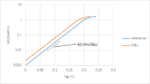
For computer vision and image processing applications there’s an edge detection algorithm called a Sobel Filter, and it’s found on Github as Open Source. The filter generates a 2D map of the gradient, and it finds the direction of largest increase from light to dark, and then rates the change in that direction. Here’s an example starting image shown on the left, the gradients, and the filtered result:
HLS Flow
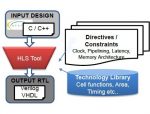
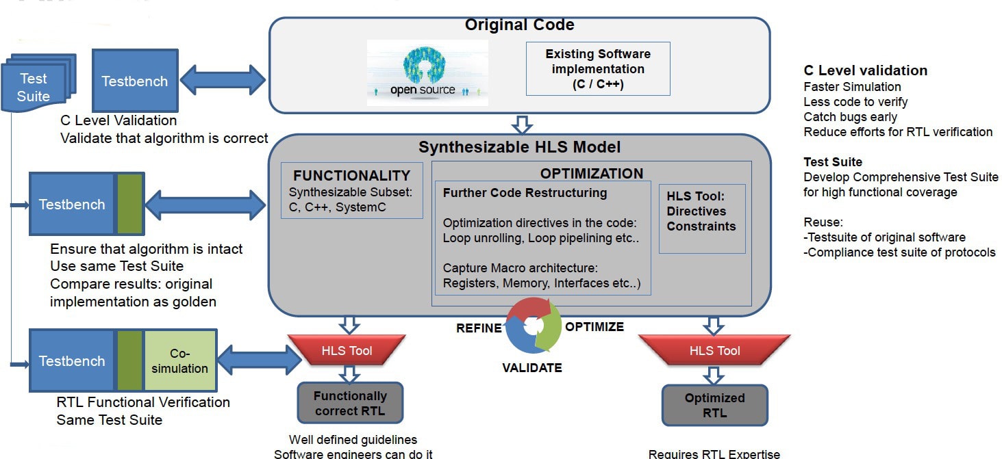
The team then modified the C code for the Sobel Filter to make it work with the synthesizable subset, then generated Verilog code using the Mentor Catapult tool.
There is a comprehensive and well defined set of guidelines for using a synthesizable subset of C / C++ / SystemC which needs to be followed. The important points of these guidelines are listed below:
- HLS tool parse the code to extract the design intent, and the entire functionality should be extractable at compile time. Any functionality that is determined at run time cannot be extracted by the tool. Constructs must be unambiguous and of fixed size.
- C functions synthesize into RTL blocks, and function arguments synthesize to RTL I/O. Arrays in the C code synthesize to memory: RAM / ROM / FIFO.
- Datatypes of the variables impact the precision, area and performance of the RTL. A generic 32bit integer can be avoided if a 10 bit integer is sufficient. HLS tool vendors provide their own implementation of datatypes for usage in synthesizable code. The Algorithmic C datatypes (AC datatypes) from Mentor Graphics were used in this exercise.
- The synthesizable code cannot use function calls from other libraries which are not synthesizable, you need to find a corresponding synthesizable library or implement it yourself. The math.h functions used in the code were replaced with the corresponding function calls from the ac_math.h / ac_dsp.h from Mentor Graphics.
Not all C / C++ constructs can be synthesized. You should avoid memory allocation, OS system calls, function pointers, STL classes, non const global variables, utility libraries etc..
One of the benefits of the proposed methodology is to reuse the test suite of the original software implementation to verify the final RTL implementation.
Most of the time, the original software implementation will have a comprehensive functional test suite, if not it will be a good idea to start by creating such a test suite. At this stage, the code base is smallest and execution speed is fastest, so comprehensive functional verification at this stage requires minimal efforts
After refining the source code to make it compliant with the synthesizable subset, you re-use the same test suite to ensure that functionality is still intact. The synthesizable code is still C / C++ code which can be compiled using gcc compiler, and does not require any specific tool set or specialized setup to take it through the original test suite. Some minor updates in the testbench may be required. It will be good to use the original software implementation as the golden reference to verify the synthesizable implementation.
Next, you synthesize the refined implementation using the HLS tool to generate RTL. For the functional verification of the RTL it is advisable to re-use the same original test suite and use the original software implementation as the golden reference. So, you can very quickly ascertain that the resulting RTL is functionally correct. This kind of setup will require Verilog-C/C++ co-simulation, and Mentor Catapult provides the SCVerify flow for verification setup.
A testbench was created to validate that the algorithm is working properly, and that testbench can be used at both the C++ and RTL levels.
With the flow explained so far, software experts can easily take the original software implementation and generate functionally correct RTL, without requiring in-depth knowledge of RTL. They just need to understand the synthesizable subset.
The RTL generated with these steps will be functionally correct, however will definitely not be in the usable form yet, as it is not fully optimized for the specific target implementation (FPGA / ASIC / technology nodes) or for specific target application requiring certain Power Performance Area matrix. To get the optimized RTL, you will have to play with the HLS tool directives and constraints, and may have to further refine the synthesizable code by using optimization directives or tool pragmas at the right places. It also requires re-structuring of synthesizable code to capture a bit of macro architecture = Registers, Memory, Interfaces etc.. This exercise requires strong understanding of the RTL, and cannot be done by software experts. The good news is that by now you already have a robust functional verification setup, and with each optimization iteration you can quickly ascertain that the implementation (C as well as RTL) is still functionally correct. This cycle of refine – optimize – verify continues till you get the final RTL that meets requirements.
Open Source HLS Libraries
Software developers generally have access to lots of free general purpose libraries, however these cannot be readily used in the synthesizable code. You need to find a corresponding HLS library, or implement it yourself as per synthesizable subset. Few HLS libraries come bundled with HLS tools , but there are a few open source HLS libraries available:
- Open source libraries from Xilinx
- Open source libraries from Mentor Graphics
- Others
Xilinx provides an HLS tool named Vivado that is widely used in the FPGA community to implement the designs at a higher abstraction level using C / C++ / SystemC. The HLS libraries provided by Xilinx works with their HLS tool, but not with Mentor Catapult and other tools. The HLS libraries provided by Mentor Graphics work with Catapult only, so it is recommended to write the synthesizable code in a tool independent fashion, so that same code can be easily re-used across multiple projects targeted for different technologies (FPGA, ASIC / SoC). There are some minor differences in how the synthesizable code has to be written for different tools. The article ‘Porting Vivado HLS Designs to Catapult HLS Platform’, provides a good summary of differences in writing code for Xilinx Vivado and Mentor Catapult. The CircuitSutra team used these concepts to migrate some of the open source Vivado HLS libraries to work with Mentor Catapult.
CircuitSutra is also in the process of developing tool independent HLS libraries corresponding to widely used software libraries.
Advanced ESL Flows
The methodology under consideration opens the door for various advanced ESL flows that were mostly a wish list.
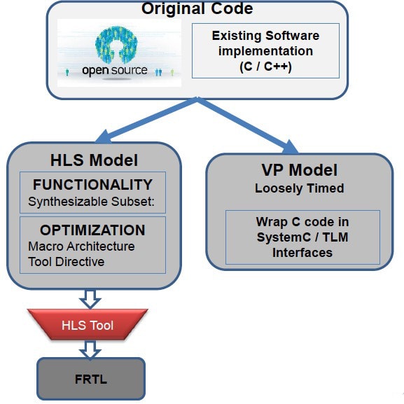
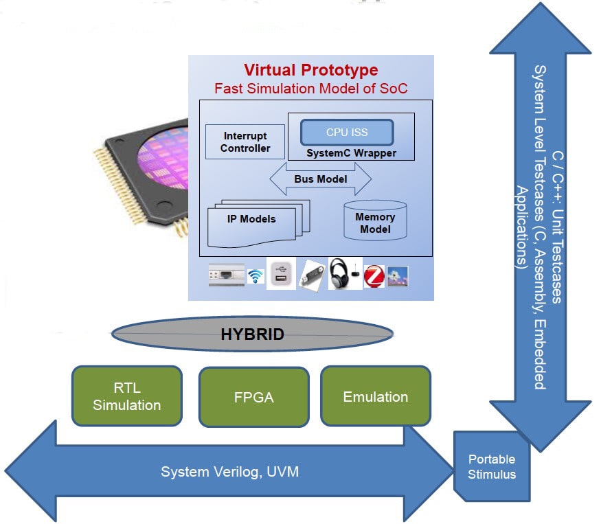
Apart from High-Level Synthesis, the other widely used use-case of ESL methodologies is virtual prototyping. Virtual prototypes are the fast simulation of models for SoCs and systems. These are used for pre-silicon, embedded software development, SoC level & System level co-design and co-verification, automated unit testing of firmware, architecture exploration etc.. Virtual Prototyping uses a CPU Instruction Set Simulator (ISS) along with IP models and memory models The models for virtual prototypes are developed using SystemC, which is a C++ library.
There has always been talk in the industry to have a single model which can be used in virtual prototypes, and also synthesized using a HLS tool to generate RTL. However both use-cases require different kinds of high level code. HLS requires code which is compliant with the synthesizable subset, virtual prototypes requires code which can simulate as fast as possible. Virtual prototype models uses the concepts like Transaction Level Modeling (TLM) and loosely timed (LT), and can use any constructs of C & C++.
Starting with the same original open source software implementation, you can now create models for both High-Level synthesis and virtual prototypes. While I explained how to make the code synthesizable, developing the model for virtual prototype is even simpler, you just need to wrap the software implementation in the SystemC and implement the transaction level interfaces and other macro-architecture details of the IP like registers, memory etc.. The same test suite can be used for the verification of both models.
You can also add hybrid modeling by simulating parts of your design in virtual prototype, RTL simulation, FPGA chips or emulator boxes.
A virtual prototype enables verification at the SoC level using bare metal tests, firmware embedded application. For maximum productivity and re-usability, you can move step by step. As a first step, run these tests on the pure virtual prototype having TLM models of IP. In the next step, you can replace the TLM version of a specific IP block with the synthesizable version of C / C++ / SystemC implementation and verify it with the same test suite. Finally, through co-simulation you replace the specific IP block with the RTL implementation and verify it with the same test suite. With each step you are moving to the slower simulation, and the objective is to catch as many bugs as possible early in the cycle when simulation is fast.
The RTL IP have to be thoroughly verified using SystemVerilog and a UVM environment. The same environment can be used to further verify the TLM models and synthesizable models. This will ensure complete equivalence at all abstraction levels.
These advanced flows are also likely to enable the effective usage of the upcoming standard Portable Stimulus, which allows you to generate different flavors of test cases from the same verification intent.
Summary
HLS is a proven approach for ESL design, and moving up from RTL coding to HLS will give you time to actually explore the design space and make early trade-offs. Because SW is written in C and C++, you can simulate both SW and early HW together early, always a good thing instead of waiting for silicon to arrive. Virtual Platforms allow you to decide what goes into SW and HW.
Companies like CircuitSutra have deep experience using these ESL approaches to implement new design products quickly and correctly.
About CircuitSutra
CircuitSutra is an Electronics System Level (ESL)design IP and services company, headquartered in India, having development centers in Noida and Bangalore, and an office in Santa Clara CA. It enables customers to adopt advanced methodologies based on C, C++, SystemC, TLM, IP-XACT, UVM-SystemC, SystemC-AMS, Verilog-AMS. Its core competencies include Virtual Prototype (Development, Verification, Deployment), High-Level Synthesis, Architecture & Performance modeling, SoC and System-Level co-design and co-verification.
CircuitSutra’s mission is to accelerate the adoption of ESL methodologies in the Industry.
CircuitSutra provides best in class ESL experts, who works as an extension of customer’s R&D team, either remotely through offshore development center (ODC) model or onsite at customer location. CircuitSutra provides re-usable modeling IP & methodology, that helps the customers to quick start their modeling projects. It also provides specialized SystemC training that helps customers to groom the non-SystemC professionals to become virtual prototyping experts.
Related Blogs


