EUV (Extreme UltraViolet) lithography has received attention within the semiconductor industry since its development inception in 1997 with the formation of the EUV LLC [1], and more recently, since the 7nm node began, with limited use by Samsung and TSMC being touted as key advantages [2, 3]. As with any key critical technology, the devil is in the details.
While much has been written about the stochastic aspects of EUV [4-8], which are troublesome in terms of defects, or the infrastructure aspects, including pellicles [9] and hydrogen cleaning [10], the imaging aspects have often been taken to be granted. Less frequently, the details of the image formation in the resist are covered. The EUV-generated image is actually produced by chemical reactions triggered by electrons released by the EUV radiation [11, 12]; these electrons would have traveled a random number of nanometers before finally fixing the reaction location. However, even the optical image projection is a key departure from mainstream DUV (Deep UltraViolet) systems which have been in use for over two decades.
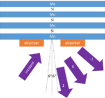
EUV is absorbed by all materials, so it is not feasible to make lenses for EUV. One mm of glass or even a thin silicon wafer would absorb all the EUV light, for example. So instead, EUV light can only be reflected using multilayers, and even here it is already partially absorbed, roughly 30% per multilayer. A fundamental consequence of relying on reflections for imaging is that the light path and its axis must be folded to avoid obstructions. The circuit layer pattern is projected from a mask into a wafer. On the mask, the features are 4x larger than the target size on the wafer, and the light is illuminated with a range of angles centered around 6 degrees with respect to the normal to the surface (Figure 1).
The amount of light reflected from the mask surface is itself a function of the angle as well as the wavelength [13]. The EUV light is commonly represented as a 13.5 nm wavelength, but it is actually a wide band of wavelengths. A longer wavelength has a higher reflectance at smaller angles with respect to the normal, while a shorter wavelength has a higher reflectance at angles further away from the normal [13, 14]. Even though the illumination distribution is centered or balanced about the optical axis (which is 6 degrees with respect to the normal), the angular dependence means, for a given wavelength, most of the light will be reflected toward one side. This produces a deviation from telecentricity, so that the object will tend to shift when out of focus.
Figure 1. Illumination configuration for the EUV mask. The circuit layer pattern is defined in an absorber. When the absorber is laid out on a fixed pitch, as in a grating, the light is reflected along specific direction, each labeled as a diffraction order.’0′ marks the direction for a blank pattern, i.e., pure specular reflection.
What is not so commonly mentioned, though, is that the EUV mask itself contributes additional anomalies to the imaging. It is a combination of two effects [15]. The EUV mask can be modeled as paterned layer covering the reflective multilayer, consisting of “bright” and “dark” areas. The “bright” areas have the multilayer surface exposed and available for reflecting while the “dark” areas are covered by an absorber consisting (at least in part) of tantalum. The “dark” areas on the EUV mask still reflect light since the (~60 nm thick) absorber still transmits light through to the multilayer underneath. After reflecting back, ~3% of the light is allowed to proceed to the rest of the optical system. This light, however, is shifted in phase (~150 degrees) with respect to the light that did not pass through any absorber. So instead of a black-and-white pattern, it’s more like an oil pattern on glass. It should also be borne in mind that this “dark” phase shift is also inversely proportional to the wavelength.
Figure 2 shows the impact of the phase shift on the image position. The 1:1 line-space image is assumed to be defined by just the 0th and 1st orders. For a 180 degree phase shift, there is no change of position, but for phase shifts that depart from 180 degrees, toward 90 degrees, the image begins to shift. Beyond 90 degrees, it starts shifting back, until it reaches the original position at 0 degrees.
Figure 2. The phase of the 3% dark space affects the CD as well as the position of the bright dense line image. The shift is zero for 0 and 180 degrees, and is maximized at 90 degrees. For a 20 nm line on 40 nm pitch, this can be in the 1-2 nm range. Going from 180 degrees to 0, the image peak intensity and width also grows.
The phase shift effect cannot be sufficiently compensated by optical proximity correction (OPC). With the 150 degree phase shift and 3% reflected through absorber, 20 nm linewidths on 40 nm and 80 nm pitches are compared in Figure 3, along with OPC by sizing alone as well as with sizing + subresolution assist features (SRAFs) [16].
Figure 3. With unbalanced illumination, a 20 nm dense line image (40 nm pitch) is shifted from its presumed position by 2-3 nm with the dark space transmitting 3% at a phase of 150 degrees. At 2X pitch, the shift is even larger, and not even OPC can correct it to match the dense line case. The vertical dashed lines mark the peak centers for the 40 nm pitch and 80 nm pitch (sizing + assist features) cases.
The 80 nm pitch is formed with 0th, 1st and 2nd diffraction orders. While the 0th and 2nd orders can correlate with the 0th and 1st orders of the 40 nm pitch, the 1st order of the 80 nm pitch will always pose an unremovable difference between the two pitches, and so cannot complete the optimization, even with the use of subresolution assist features. Moreover, when the phase is not 180 or 0 degrees, sizing the feature cannot improve the contrast, i.e, the sharpness of the edge slope. While the assist feature helps mitigate the shift to some degree, it does so by suppressing the 1st order, which also reduces the peak intensity and worsens the contrast. In practice, the imaging situation would not be as dire as in Figure 3, because there is partial balancing around the optical axis, just not complete balance.
On the other hand, the image shift gets worse when defocus is considered, and in fact, the best focus positions for different pitches can span a wide range [15, 17, 18]. Moreover, for the different wavelengths from the EUV source, each wavelength has a different phase shift independent of the others. As a result, overlay is a concern, when the spec is on the order of 1.5 nm [19]. ASML has also alluded to this vulnerability of EUV [20].
The underlying phase shift issue is fundamentally part of the EUV mask itself. So the solution requires a redefinition of the EUV mask. More specifically, the phase shift could be made zero by picking an absorber whose index of refraction has a real component of 1, while at the same time maintaining a sufficiently high absorption coefficient [15, 21, 22]. The most promising candidates have been based on nickel, including nickel-aluminum alloy, or nickel nanoparticles embedded in tantalum nitride [21-23], although these materials have been hard to process [23]. Other considered candidates include telluride-based, which is less stable chemically, and ruthenium-based, which deviates more from the desired optical properties [21, 24]. Challenges linger in being able to pattern these fairly exotic materials [24].
References
[1] https://www.latimes.com/archives/la-xpm-1997-sep-11-fi-31072-story.html
[2] https://news.samsung.com/global/samsung-electronics-starts-production-of-euv-based-7nm-lpp-process
[3] https://www.anandtech.com/show/13445/tsmc-first-7nm-euv-chips-taped-out-5nm-risk-in-q2
[4] P. De Bisschop and E. Hendrickx, “Stochastic Effects in EUV Lithography,” Proc. of SPIE 10583, 105831K (2018).
[5] M. Neisser et al., “Understanding EUV Shot Noise: Comparing Theory and Requirements to Experimental Evidence,” J. Photopoly. Sci. Tech. 26, 617 (2013).
[6] https://www.linkedin.com/pulse/euvs-stochastic-valley-death-frederick-chen/
[7] https://www.linkedin.com/pulse/stochastic-variation-euv-source-illumination-frederick-chen/
[8] https://www.linkedin.com/pulse/photon-shot-noise-impact-line-end-placement-frederick-chen
[9] O. Romanets et al., “Progress in imaging performance with EUV pellicles.” Proc SPIE 11177, 111770Z (2019).
[10] https://www.linde-gas.com/en/images/SST%20-%20March%202018%20-%20EUV%20Lithography%20Adds%20to%20Increasing%20Hydrogen%20Demand%20at%20Leading-edge%20Fabs_tcm17-477308.pdf
[11] H. Fukuda, “Localized and cascading secondary electron generation as causes of stochastic defects in extreme ultraviolet projection lithography,” J. Micro/Nanolith. MEMS MOEMS 18(1), 013503 (2019).
[12] I. Bespalov et al., “Key Role of Very Low Energy Electrons in Tin-Based Molecular Resists for Extreme Ultraviolet Nanolithography,” ACS Appl. Mater. Interfaces 12, 9881 (2020).
[13] https://www.linkedin.com/pulse/very-different-wavelengths-euv-lithography-frederick-chen
[14] N. Davydova et al., “EUVL mask performance and optimization,” Proc. SPIE 8352, 835208 (2012).
[15] M. Burkhardt and A. Raghunathan, “Best focus shift mechanism for thick masks,” Proc. SPIE 9422, 94220X (2015).
[16] J. G. Garofalo et al., “Automated layout of mask assist-features for realizing 0.5 k1 ASIC lithography,” Proc. SPIE 2440, 302 (1995).
[17] A. Erdmann et al., “Mask-induced best-focus shifts in deep ultraviolet and extreme ultraviolet lithography,” J. Micro/Nanolith. MEMS MOEMS vol. 15(2), 021205 (2016).
[18] A. Erdmann et al., “Characterization and mitigation of 3D mask effects in extreme ultraviolet lithography,” Adv. Opt. Tech. vol. 6(3-4), 187 (2017).
[19] https://www.asml.com/en/products/euv-lithography-systems/twinscan-nxe3400c
[20] https://www.fool.com/earnings/call-transcripts/2020/04/15/asml-holding-nv-asml-q1-2020-earnings-call-transcr.aspx
[21] A. Erdmann et al., “Attenuated PSM for EUV: Can they mitigate 3D mask effects?,” Proc. SPIE 10583, 1058312 (2018).
[22] V. Luong et al., “Ni-Al Alloys as Alternative EUV Mask Absorber,” Appl. Sci. 8, 521 (2018).
[23] D. Hay et al.,”Thin Absorber EUV Photomask Based on Mixed Ni and TaN Material,” Proc. SPIE 9984, 99840G (2016).
[24] V. Philipsen et al., “Novel EUV mask absorber evaluation in support of next-generation EUV imaging,” BACUS News, October 2019.