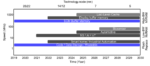
webinar banner AI 2026 v2

Multi-Vt Device Offerings for Advanced Process Nodes

Multi-Vt Device Offerings for Advanced Process Nodes
by Tom Dillinger on 06-26-2020 at 6:00 am

Ion Ioff

Summary
As a result of extensive focus on the development of workfunction metal (WFM) deposition, lithography, and removal, both FinFET and gate-all-around (GAA) devices will offer a wide range of Vt levels for advanced process nodes below 7nm.

Introduction
Cell library and IP designers rely on the availability of nFET and pFET devices with a range of threshold voltages (Vt).  Optimization algorithms used in physical synthesis flows evaluate the power, performance, and area (PPA) of both cell “drive strength” (e.g., 1X, 2X, 4X-sized devices) and cell “Vt levels” (e.g., HVT, SVT, LVT) when selecting a specific instance to address timing, noise, and power constraints.  For example, a typical power optimization decision is to replace a cell instance with a higher Vt variant to reduce leakage power, if the timing path analysis margins allow (after detailed physical implementation).  The additional design constraints for multi-Vt cell library use are easily managed:  (1) the device Vt active area must meet (minimum) lithography area requirements, and (2) the percentage of low Vt cells used should be small, to keep leakage currents in check.

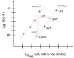
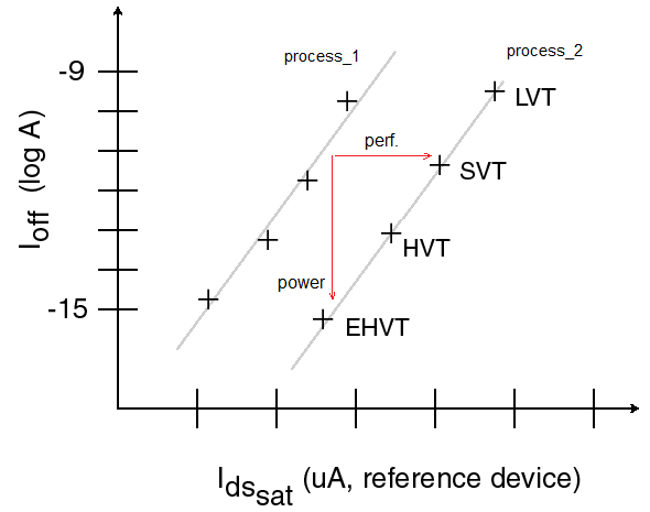
A common representation to illustrate the device Vt offerings in a particular process is to provide an I_on versus I_off characterization curve, as shown in the figure below.

Although it doesn’t reflect the process interconnect scaling options, this curve is also commonly used as a means of comparing different processes, as depicted in the figure.  A horizontal line shows the unloaded, I_on based performance gains achievable.  The vertical line illustrates the iso-performance leakage I_off power reduction between processes, for a reference-sized device in each.  Note that these lines are typically drawn without aligning to specific (nominal) Vt devices in the two process nodes.

The I_on versus I_off curve does not really represent the statistical variation in the process device Vt values.  A common model for representing this data is the Pelgrom equation. [1]  The standard deviation of (measured) device Vt data is plotted against (1 / sqrt(Weff * Lgate)):

(sigma_Vt)**2 =  (A**2) / 2 * Weff * Lgate 

       where A is a “fitting” constant for the process

Essentially , as the square root of the channel area of the device is increased, the sigma-Vt decreases.  (Consider N devices in parallel with independent Vt variation – the Vt mean of the total will be the mean of the Vt distribution, while the effective standard deviation is reduced.)  The Pelgrom plot for the technology is an indication of the achievable statistical process control – more on Vt variation shortly.

For planar CMOS technologies, Vt variants from the baseline device were fabricated using a (low impurity dose) implant into the channel region.  A rather straightforward Vt implant mask lithography step was used to open areas in the mask photoresist for the implant.  For an implant equivalent to the background substrate/well impurity type, the device Vt would be increased.  The introduction of an implant step modifying the background concentration would increase the Vt variation, as well.

With the introduction of FinFET channel devices, the precision and control of implant-based Vt adjusts became extremely difficult.  The alternative pursued for these advanced (high-K gate oxide, metal gate) process nodes is to utilize various gate materials, each with a different metal-to-oxide workfunction contact potential.

Vt offerings for advanced nodes
As device scaling continues, workfunction metal (WFM) engineering for Vt variants is faced with multiple challenges.  A presentation at the recent VLSI 2020 Symposium by TSMC elaborated upon these challenges, and highlighted a significant process enhancement to extent multi-Vt options for nodes below 7nm. [2]

The two principal factors that exacerbate the fabrication of device Vt’s at these nodes are shown in the figures below, from the TSMC presentation.

  • The scaling of the device gate length (shown in cross-section in the figure) requires that the WFM deposition into the trench be conformal in thickness, and be thoroughly removed from unwanted areas.
  • Overall process scaling requires aggressive reduction in the nFET to pFET active area spacing.  Lithographic misalignment and/or non-optimum WFM patterning may result in poor device characteristics – the figure above illustrates incomplete WFM coverage of the (fin and/or GAA) device.

Parenthetically, another concern with the transition to GAA device fabrication is the requirement to provide a conformal WFM layer on all side of each (horizontal) nanosheet, without “closing off” the gap between sheets.

The TSMC presentation emphasized the diverse requirements of HPC, AI, 5G comm., and mobile markets, which have different top priorities among the PPA tradeoffs.  As a result, despite the scaling challenges listed above, the demand for multi-Vt cell libraries and PPA optimization approaches remains strong.  TSMC presented extremely compelling results of their WFM fabrication engineering focus.  The figure below illustrates that TSMC has demonstrated a range of Vt offerings for sub-7nm nodes, wider than 7nm.  TSMC announced an overall target Vt range exceeding 250mV.  (Wow.)

In addition to the multi-Vt data, TSMC provided corresponding analysis results for the Vt variation (Pelgrom plot) and the time-dependent device breakdown (TDDB) reliability data – see the figures below.

The sigma-Vt Pelgrom coefficient is improved with the new WFM processing, approaching the 7nm node results.  The TDDB lifetime is also improved over the original WFM steps.

The markets driving the relentless progression to advanced process nodes have disparate performance, power, and area goals.  The utilization of multi-Vt device and cell library options has become an integral design implementation approach.  The innovative process development work at TSMC continues this design enablement feature, even extending this capability over the 7nm node – that’s pretty amazing.

For more information on TSMC’s advanced process nodes, please follow this link.

-chipguy

References
[1]  ] M. J. M. Pelgrom, C. J. Duinmaijer, and A. P. G. Welbers, “Matching properties of MOS transistors”, IEEE J. Solid-State Circuits, vol. 24, no. 5, pp. 1433–1440, Oct. 1989.

[2]  Chang, Vincent S., et al., “Enabling Multiple-Vt Device Scaling for CMOS Technology beyond 7nm Node”, VLSI Symposium 2020, Paper TC1.1.

Images supplied by the VLSI Symposium on Technology & Circuits 2020.


Nobody Ever Lost Their Job for Spending too Much on Hardware Verification, Did They?

Nobody Ever Lost Their Job for Spending too Much on Hardware Verification, Did They?
by Daniel Nenni on 06-25-2020 at 6:00 am

Silicon Bug Cost Scenario

A paper was published last month on the Acuerdo Consultancy Services website authored by Joe Convey of Acuerdo and Bryan Dickman of Valytic Consulting. Joe and Bryan spent combined decades in the Semi and EDA World which means they have a great understanding of hardware bugs first hand, absolutely.

Here is a quick summary with a link to get the full paper at the end:

Whether you are developing a hardware product or a software product or both, understanding bugs, what causes them, how to avoid them, the cost of finding them and the cost of not finding them, becomes one of the biggest drivers that shape how teams develop products. Understanding all aspects of this will help you to reason about the balance between delivered product quality and ROI; too much or too little?

Economics of Bugs
In IP hardware product development, bugs drive a large part of the development cost and getting the investment balance wrong will have a big impact. How do teams deliver on time, with functionality, performance and integrity and what are the costs involved in ensuring an absence of bugs and the delivery of high-quality products?

Getting the investment vs risk balance right is hard…

Nobody wins if a design team get it wrong. Market reality means that costs will often be passed down the customer/consumer food chain and eventually impact end-users. Bug escapes can drive up mitigation and development costs and subsequently drive down ROI and customer confidence.

How to get the balance between investing too little (with unacceptably high risk), versus “too much” (low risk, but lousy ROI) is a long-standing challenge that design teams and the CFO have to grapple with. Engineering usually win the investment battle with the CFO, because few in senior management challenge the assertion that “you can never spend too much on finding bugs”. This results in a spiraling investment in compute and EDA tools as designs get more complex. Sound familiar?

People are your most valuable asset
The success of the products comes down to the quality of the staff; how well trained they are; how experienced they are and how innovative they are; how well equipped they are with the ‘best-in-class’ tools and resources to do their jobs. Engineers love to solve challenging problems, innovate, build ‘cool’ things, be experts and craftsmen, have access to the latest and best-in-class platforms and tools and work with teams of talented colleagues. Do they really understand how much this costs?

Get engineering teams on-side by growing a shared understanding of engineering platform costs
An interesting challenge for any business developing complex products that consume costly tools and resources is how to educate engineering teams to be cost-conscious and use the available resources sparingly and effectively. Of course, engineers understand cost, but providing the teams with clear data showing the relationship between the cost of providing the engineering platform and the process of designing IP can create positive perspectives on how to create cost efficiencies;

Wow, did we really spend that much? Surely, we can do something about that by improving xyz?

A huge part of improving product ROI is the drive for design efficiencies. Sharing the business challenge can provide a very positive environment to encouraging innovations in methodologies and deployment of tools, at a cost profile that fits the company’s business plans and provides engineering best in class facilities.

Work with engineering to drive great partnerships with EDA and other platform vendors
Having engineering as a willing partner makes a difference to the success of tool evaluations and subsequent negotiations with vendors. Creating a culture of partnership that transcends internal barriers but also extends to the company’s EDA and IT suppliers is really valuable, as it encourages vendors to become “partners” working with engineering in a joint effort to confront the technical challenges involved in a process like IP verification and debug.

Compute, compute and even more compute…
We need more compute, otherwise there will be product delays and missed revenue targets… Over the last two decades the industry has seen the compute requirement for Verilog simulation grow by several orders of magnitude and the compute infrastructures have scaled up accordingly. Businesses are migrating compute capacities from on-prem to cloud, which offers much greater capacity agility and enables teams to reason better about cost versus time to delivery.

We’re going to spend more money over a shorter time and deliver earlier.

For many, this means operating a hybrid on-prem/cloud environment. EDA vendors are adapting their tools and their business models to cope with this new hybrid-cloud world.

For complex IP products such as processors, most of this simulation consumption is taken up by constrained-random verification strategies where the ability to consume cycles is open-ended.

But I ONLY want to run GOOD verification cycles!

So, when is a verification cycle a “good cycle”? Only if “Verification Progress” has been made. By that we mean that it has either found a new bug, or it has measurably increased the testing space i.e. demonstrated correctness. The former is easy to track (we can count bugs), but the latter is harder because we don’t know precisely how many bugs are present. Instead, we track endless metrics such as coverage and cycles of testing.

Extensive operational analytics are needed in order to operate a resilient and performant platform service delivering the appropriate QoS. These analytics will monitor system performance and capacities, track operational metrics over time and may exploit machine learning prediction algorithms to alert to pending failures so that mitigations can be deployed ahead of a critical failure point.

Conclusion
It boils down to understanding the total cost of bugs expressed as the costs expended in finding bugs, versus the cost of not finding bugs, i.e. what is the total impact cost when bugs are missed?

Which of the above 2 scenarios are you in? Do you have enough data to be able to reason about this and decide which scenario applies to your operations? If not, then what actions are you going to take to find out where you are and what action to take in each situation?

If your analysis shows that you are in scenario A, it looks like you need to address product quality urgently. You’re not really investing sufficiently in IP Product Verification and the impact costs are significantly reducing your products’ ROI. Scenario B certainly feels more comfortable, but you might have nagging doubts about the efficiency of your operations….

Now you have the right information to make the appropriate investments and get the balance right – and by the way, don’t lose your job!

Get the full paper “On the Cost of Bugs”.


Key Semiconductor Conferences go Virtual

Key Semiconductor Conferences go Virtual
by Scotten Jones on 06-24-2020 at 2:00 pm

IEDM 2020 Logo

This last week the 2020 Symposia on VLSI Technology and Circuits (VLSI Conference) was held as a virtual conference for the first time and it was announced today (June 24th) that this year’s IEDM conference will also be held as a virtual conference.

“The IEDM Executive Committee has decided that in the interest of prioritizing the health and safety of the scientific community, a virtual approach is the best option for this year,” said Dina Triyoso, IEDM 2020 Publicity Chair and Technologist at TEL Technology Center, America, LLC.

I attended the virtual VLSI Conference last week and I thought it would be interesting to discuss my experience with the conference and what it means for IEDM.

The first and perhaps most obvious aspect of a virtual conference is you do not have to travel to attend it saving travel expenses and time away from the office. Of course, the question then becomes what is the experience like?

In general, I really liked the experience, in fact I would say that in many ways I prefer the virtual conference.

The advantages of a virtual conference:

  • No travel, saving time and money.
  • At large conferences there are often parallel tracks with multiple papers being presented at the same time. It is not uncommon to have two or even more papers I would like to see presented at the same time. Conversely there will sometimes be gaps where there are no papers of interest being presented. For the virtual conference, the papers were live streamed and recorded. I exclusively accessed the conference through the recordings and really likes that I could pick when I wanted to watch different presentations and never had to choose one over the other because of scheduling conflicts.
  • When you are at a conference watching a paper presented, you are often sitting in a tightly packed auditorium trying to take notes on a computer in your lap and the presenter is trying to fit in as much information as possible in their time slot. It can be difficult to capture all the information. Sitting at my computer watching a video that I can pause, and rewind is a much better experience.
  • At some conferences, such as the SPIE Advanced Lithography Conference there are essentially no proceedings, at other conferences such as VLSI and IEDM the papers are published in a proceeding, but the presentations are typically not made available. The presentations often have a lot more figures than the paper and are a valuable source of additional information. At the virtual VLSI Conference as you watched each presentation you had the option of downloading the paper and the presentation.

There are some disadvantages to a virtual conference and there were some execution issues with the VLSI Conference:

  • One important part of technical conferences is the opportunity to have private conversations with colleagues and to network, that is missing from a virtual conference.
  • I heard there were some streaming issues with the conference and one of the recorded presentations I watched had the sound fading out periodically throughout the presentation. These are the kind of technical issues I would expect would get worked out with more experience with virtual conferences.
  • You had to sign in to each session and then if you want to switch to a new session sign in again, it would have been easier if you could just sign in and then navigate between sessions but this was a minor inconvenience.
  • My biggest issues with the virtual conference was the over one hundred reminders emails I was sent. It seems that each session sent a reminder in advance and if you didn’t watch the live stream you got a sorry you missed it email as well. I complained about this to the committee and was told it was a feature of the software that couldn’t be turned off (and there is no opt out link on the emails either). This needs to be fixed.

Overall, I thought it was a good experience. I even suggested to the conference that since everything is recorded, they could leave registration open for a few months and people could sign up and watch the conference and download the papers, this could potentially be a way to expand the revenue stream for the conference.

I will miss networking at IEDM this year, it is an important conference for me in that respect, but I am looking forward to a better experience accessing the technical conference through a virtual conference.

IEEE International Electron Devices Meeting (IEDM) is the world’s preeminent forum for reporting technological breakthroughs in the areas of semiconductor and electronic device technology, design, manufacturing, physics, and modeling. IEDM is the flagship conference for nanometer-scale CMOS transistor technology, advanced memory, displays, sensors, MEMS devices, novel quantum and nano-scale devices and phenomenology, optoelectronics, devices for power and energy harvesting, high-speed devices, as well as process technology and device modeling and simulation.

Also Read:

Effect of Design on Transistor Density

Cost Analysis of the Proposed TSMC US Fab

Can TSMC Maintain Their Process Technology Lead


Apple’s Silicon Switch Changes Game & Balance 

Apple’s Silicon Switch Changes Game & Balance 
by Robert Maire on 06-24-2020 at 10:00 am

Intel Apple Silicon

Will/should others follow?
TSMC vs Intel impact?
Moving Apple’s supply chain further overseas

Apples move to self served silicon was no surprise…..
It has been speculated for years and we have talked about it many times.  It makes more sense for Apple to have silicon, custom designed for their applications and products that fit exactly in their line up. Rather than use an “adapted” X86 architecture that harkens back and pays homage through compatibility to the earliest Intel CPUs, Apple can finally have a “purpose built” CPU that fulfills all its needs.

Not to mention the fact that what really sealed the deal and perhaps accelerated the need was that TSMC had passed Intel in the Moore’s law race.  Not jumping on the TSMC bandwagon would limit Apple to underperformance as compared to what is available.

Apple can gain further differentiation in the marketplace as compared to other laptop makers who really can’t differentiate themselves as they all use the same engine, Intel.

Not the first time Apple switches CPUs…
Apple has changed CPUs several times over the years as the industry has moved forward.  The change from Intel is just another sign that the industry has moved on.

Apple started, way back when, on its Apple II, with a MOS 6502 , 8 bit, CPU which was a much cheaper, better copy of the Motorola 6800 cpu and also way cheaper than Intel’s 8080. The 6502 was used in the Atari 2600 game console and Commodore consumer computer, so cost was a big factor.

The jump to Apple Macintosh also saw a jump to the Motorola 68000 CPU a 16/32 bit design.

Later on down the road, Apple switched again to the PowerPC CPU by IBM which was a RISC (reduced instruction set) CPU versus other popular CISC (Complex Instruction Set) CPUs at the time.

As Apple had its own OS and own infrastructure, X86 compatibility was not as much an issues and perhaps Apple’s “Think Different” mind set helped it go its own way.

Then back in 2005 Apple announced that it had cut a deal with Intel to move to Intel’s X86 line.  We are sure Apple goy a good deal from Intel for the switch and the PowerPC was already on its way out so Apple was jumping ship just at the right time.

Obviously Intel at the time was the CPU powerhouse and had performance that shut out everyone else due to its Moore’s law lead.

Intel’s misstep’s and slowness at entering the mobile CPU market was perhaps the beginning of the end of the relationship as Apple went its own way with ARM based CPUs that morphed into fully custom , purpose built CPUs.

Apple has spent years building up its CPU expertise by acquiring many silicon companies, pouring tons of money into R&D , hiring the best and brightest like Jim Keller, the CPU guru of Apple, AMD, Tesla and Intel.

It obviously makes more sense for Apple to similar CPUs across all its devices for a compatible, seamless product line.

The final handwriting was on the wall as TSMC seemed to pass Intel in terms of transistor density and power consumption characteristics.

Apple is also a huge company as compared to Intel, it has the critical mass, and certainly no longer needs to live within the confines of an Intel dictated architecture that suits Intels needs (and profits).

If anything, we are surprised that this didn’t happen a lot sooner

Collateral Impact, shifts supply chain further to Asia
The move obviously means that TSMC will get a lot more business.  TSMC already makes all of AMDs products that matter, many of Intels products and already makes all of Apples Iphone, Ipad, Iwatch chips.  TSMC is becoming ever more critical as the key, central linchpin to the entire US technology industry.  It is clearly a single point of failure located a short boat ride from China.

This obviously doesn’t jive well with recent problems with Huawei and makes the “token” TSMC fab proposed for Arizona look even more inadequate than before.

If anything the move by Apple further focuses things on the TSMC single point of failure to the US technology industry.

Intel impact
Apple is a large but not too large a customer.  We view the loss as expected and is more of a psychological loss than a financial numerical loss.  Losing the hottest customer in the market is obviously an embarrassment and further proof of the need of Intel to double down to regain its position in Moore’s Law.

It also says that Intel is not competitive for mobile, power sensitive applications but is better off in the data center where power consumption matters less.

Intel has been making most of its money in the data center anyway but it would be better to not lose the diversification.

Should/will others follow suit?
An interesting question now is whether other Laptop/ consumer PC makers will try to follow Apple’s lead and use custom or ARM like processors? The obvious limitation is Microsoft and Windows 10 which powers the rest of the world. Would Microsoft abandon the ancient Wintel duopoly and build a more portable Windows 11? (or whatever number)

We think that Microsoft has to be wondering if they are tied to a sinking ship.  If Apple demonstrates significant power/performance benefits by leaving Intel then it will pick up more market share, which means Microsoft will lose share.

It seems like it would at least be a cheap insurance policy for Microsoft to develop ARM like compatibility to hedge against its potential success.

Having one company, Apple, with application transportability across smart phones, tablets and laptops and wearables all with the same underlying CPU architecture will be huge. Microsoft flopped in smart phones, is lame in tablets and no where in wearables. If I were Microsoft I would be thinking hard about being tied to Intel which will be relegated to the data center only with free Linux as an alternative.

Microsoft already demonstrated PowerPoint at Apple’s roll out and we are sure the full Microsoft suite will move to Apples architecture.

What do PC makers such as Dell , Lenovo, HP and others do?

We think this is a very open ended question that begs answering.  The wrong thing to do is clear….don’t sit around continuing to do the same thing that you have done for the past ten years.

Could Apple become a chip maker?
Apple could very easily make, using TSMC, and sell a version of their CPU architecture to other hardware manufacturers.

Maybe they could sell a version not quite as capable as their own but still better in performance/power than the Intel/AMD alternatives.

They could probably sell it at a pretty good margin and give Intel and AMD a run for their money as the design would likely be better for laptops and portable applications. The bonus would be that Microsoft applications are already compatible with it.

Maybe Google would love it for a Chromebook application and get Microsoft apps to boot. Apple would not cannibalize its own sales as it would still be the only company offering the same architecture from wearables to laptops but it could create more critical mass for more applications to be ported (not that there isn’t enough demand already).

The idea of Apple selling chips is not at all that far fetched if they turn out to be that much better than Intel/AMD.

How many years is “many years to come”?
Tim Cook said that Apple will support X86 devices compatibility for “many years to come”.  In our view that could be as few as two years (the plural of year-many just means more than one….).

When Apple switched from PowerPC their support ended in 3 years after which PowerPC based devices became paperweights.

We think Apple will dump Intel as fast as possible.  Its great for Apple as they get to sell a lot of new laptops at better margins.

For me as a consumer, I will run out and buy a new Apple CPU based laptop as soon as they are available as I would love to have application transportability across my Iphone/Ipad/Iwatch.  I think this clearly expands the addressable market for Apple laptops as many people would switch from windows to get that compatibility.

It will be a seismic change for not just Apple.

The Stocks
There is zero near term impact but just more things to track going forward to watch the transition play out.  Apple has had a lot of time to plan this and won’t screw it up.  It will likely be faster/better than expected.  It is broadly, long term positive for Apple and broadly long term negative for Intel.

It does not impact chip equipment in that it is a zero sum game.  It does obviously benefit TSMC who gains even more leverage and dominance in the market.

We wonder when the administration and legislators will pick up on this acceleration of outsourcing to Asia.

Semiconductor Advisors

Semiconductor Advisors on SemiWiki


Why Go Custom in AI Accelerators, Revisited

Why Go Custom in AI Accelerators, Revisited
by Bernard Murphy on 06-24-2020 at 6:00 am

frame interpolation

I believe I asked this question a year or two ago and answered it for the absolute bleeding edge of datacenter performance – Google TPU and the like. Those hyperscalars (Google, Amazon, Microsoft, Baidu, Alibaba, etc) who want to do on-the-fly recognition in pictures so they can tag friends in photos, do almost real-time machine translation, and many other applications. But who else cares? I’ve covered a couple of Mentor events on using Catapult HLS to build custom accelerators. Fascinating stuff and good insights to the methods and benefits, but I wanted to know more about what kind of applications are using this technology.

I talked to the Catapult group to get some answers: Mike Fingeroff (technologist for Catapult), Russ Klein (Product Marketing for Catapult) and Anoop Saha (Senior manager, strategy and Biz Dev for machine learning and 5G).

Video Interpolation

Anoop talked about one very cool application – video frame interpolation. You take a video at some relatively low number of frames per second, say 20 fps, but maybe you want to play it back on a 60fps display. Maybe you also want to replay in slow-motion. In either case you have gaps between frames which must be filled in somehow if you don’t want a jumpy replay. The simple answer is to average between frames. But that’s pretty low quality – it looks flickery and unnatural. A much better approach today is AI-based. Train a system with (many) before and after frames to learn how to much more smoothly and more naturally interpolate. The results can be quite stunning.

5G

Anoop added that generally, any case where you have to respond to serious upstream bandwidth and be able to make near real-time decisions to influence downstream behavior, you’re going to need custom solutions to meet that kind of performance. For example, Qualcomm talks about how AI in the 5G network will help with user localization, efficient scheduling and RRU utilization, self-organizing networks and more intelligent security, much of which demands fast response to high volume loads.

Video doorbell

Russ talked about his Ring doorbell. He doesn’t want the doorbell to go off at 3am because it detected a cat nearby. He wants accurate detection at a good inference rate, but it has to be very low power because the doorbell may be running on a battery. I could imagine a similar point being made for an intelligent security system. The movie trope of detectives fast forwarding through hours of CCTV video may soon be over. A remote camera shouldn’t upload video unless it sees something significant, because uploads burn power at the camera and because who wants to scroll through hours of nothing interesting happening?

The advantage of HLS for custom AI accelerators

Fair points, but why not run this stuff on a standard AI accelerator? The Catapult team told me that their customers still see enough opportunity in the rapidly evolving range of possible AI architectures to justify differentiation in power, performance and cost through custom solutions. AI accelerators haven’t yet boiled down to a few standard solutions that will satisfy all needs. Perhaps they never will. A custom solution is even more attractive when you can prototype a system in an FPGA, refine it and prove it out, before switching to an ASIC implementation when the volume opportunity becomes clear.

Russ wrapped up by adding that algorithms are the starting point point for all these evolving AI solutions, which make them natural fit with HLS. Put that together with HLS ability to incrementally refine implementation architecture to squeeze out the best PPA (as Russ showed in an earlier webinar I blogged). Further add HLS ability to support system verification in C against very large data sets (video, 5G streams, etc). Put that all together and Russ sees the combination continuing to reinforce interest in the Catapult solution. Difficult to argue with that.

You can learn more about Catapult HERE.


How to Grow with Poise and Grace, a Tale of Scalability from ClioSoft

How to Grow with Poise and Grace, a Tale of Scalability from ClioSoft
by Mike Gianfagna on 06-23-2020 at 10:00 am

Screen Shot 2020 05 10 at 1.06.27 PM

ClioSoft published a white paper recently entitled Best Practices are the Foundations of a Startup. The piece discusses the needs and challenges associated with building a scalable infrastructure to support growth.

Before I get into more details on ClioSoft’s white paper, I would offer my own experience on this topic – the need to build a chip company with scale in mind is absolutely critical. I will draw on my experience at eSilicon.  I was one of the first employees at the company, so I had a front-row seat to watch the company’s growth.  And grow we did, from a modest mainstream ASIC suppler to an advanced 2.5D FinFET ASIC supplier, building some of the most complex chips in the world.

There are many parts of this story. I will focus briefly on just one – the compute infrastructure for chip design and tapeout. In the early days, eSilicon operated its own compute farm, first on-site and then at a co-located facility not far from its headquarters in the Bay Area. We owned the computers and managed the whole thing in house. For the types of chips we were doing, this strategy was predictable and effective.

As we began to grow and move from mainstream designs to cutting-edge FinFET and 2.5D designs, it became clear the “owner/operator” model was going to break. The advanced chips we were contemplating required at least 10X more compute resources, often a lot more than that near tapeout. We couldn’t afford to buy all that gear. And even if we could, hiring enough people to manage a facility like that would be daunting.

The company attacked the problem in two parts.  First, we outsourced our data center operation and the management of it to a large service provider who did that kind of thing all the time.  Our un-manageable capital and manpower problem was now a manageable operating expense problem. Later on, we saw the additional benefits of moving to the cloud, so we did that to further manage expense and allow massive on-demand bursts of compute during tapeout. By staying ahead of the need, our infrastructure was able to scale with the company. I’d like to give a shout-out to the long-time CIO at eSilicon who had the foresight to stay ahead of the curve – Naidu Annamaneni.

Back to the ClioSoft white paper. This discussion treats compute infrastructure scalability as well as design methodology scalability.  The reasons to adopt best practices are explained well. The piece also spends some time on the design management aspects of the problem.  This one has multiple dimensions. Storing and managing design data are part of it of course.

The white paper makes a compelling case for getting collaboration tools such as design data management correct at the beginning of a company’s life. The need for simplicity and agility are also addressed. To whet your appetite, here are some of the topics covered:

  • Naming conventions
  • Data storage and backup conventions and processes
  • Design flows and handoffs
  • Design management tools and methodology
  • Issue tracking and other collaboration tools
  • Project and schedule management

You can access the new ClioSoft white paper here. Happy reading.

ClioSoft was launched in 1997 by Srinath Anantharaman as a self-funded company, with the SOS design collaboration platform as its first product. The objective then, was to help manage front end flows for SoC designs.

The SOS platform was later extended to incorporate analog and mixed-signal design flows wherever Cadence Virtuoso® was predominantly used. SOS is currently integrated with tools from Cadence®, Synopsys®, Mentor and Keysight Technologies®. ClioSoft also provides an enterprise IP management platform for design companies to easily create, publish and reuse their design IPs called designHUB.

Today ClioSoft, driven by the experience and innovation of a number of engineers, is the market leader for design data and IP management solutions and the #1 choice for analog and mixed-signal designers.

Also Read

How to Modify, Release and Update IP in 30 Minutes or Less

Best Practices for IP Reuse

WEBINAR REPLAY: AWS (Amazon) and ClioSoft Describe Best Cloud Practices


Design Technology Co-Optimization (DTCO) for sub-5nm Process Nodes

Design Technology Co-Optimization (DTCO) for sub-5nm Process Nodes
by Tom Dillinger on 06-23-2020 at 6:00 am

scaled metal resistance

Summary
Design Technology Co-Optimization (DTCO) analysis was pursued for library cell PPA estimates for gate-all-around (GAA) devices and new metallurgy options.  The cell design and process recommendations are a bit surprising.

Introduction
During the “golden years” of silicon technology evolution that applied Dennard scaling, the tasks of fabrication process development and library circuit design were rather disjoint.  Physical and electrical models for scaled devices and interconnects were derived and IP design progressed while the process was being qualified.  The development of “contactless” local FEOL metallization and the transition to damascene Cu BEOL interconnects introduced some additional considerations – yet, process bring-up and IP design were still relatively distinct.

Several factors led to the need for a much closer collaboration between process and library development, a partnership which has been described as “design technology co-optimization” (DTCO):

  • The end of Dennard scaling (around 2006) required that the physical layout design rules for device and interconnect fabrication were each individually optimized. The drawn-to-electrical device dimension bias became an integral part of establishing circuit density and performance targets.
  • The slowing of supply voltage scaling meant that the reductions in device current and device power were not keeping up with the physical density improvements. (The increasing contribution of device sub-threshold leakage currents exacerbated the problem.)  Circuit library design needed to accommodate power distribution network (PDN) optimizations that addressed I*R and L*di/dt voltage drop concerns.
  • The quantization of device dimensions associated with the introduction of FinFET technology further complicated library IP physical and electrical design. Cell dimensions were established to provide for a discrete number of nFET and pFET fins.  Additionally, diverging markets results in the bifurcation of IP library design, into high-performance and high-density variants.

The figure below illustrates a “typical” 6-track (6T) cell definition, with four internal first metal signal wiring tracks and 2X-wide power and ground rails shared between abutting (flipped) cell rows for the PDN.

Figure 1.  Cross-section of 6T cell, in a FinFET technology.  (Source:  Synopsys)

In all these cases, DTCO was necessary for process and IP development (and for the subsequent introduction of enhanced process variants at the same physical node).

Recent DTCO Analysis

Fast-forwarding to the present…

At the recent VLSI 2020 Symposium on Circuits and Technology, a prevalent theme was the transition from FinFET to gate-all-around (GAA) “nanosheet” devices.

A team from Synopsys and Applied Materials provided an invited talk with compelling data from their DTCO analysis of GAA-based cell library design for sub-5nm nodes. [1]  I found their analysis to be extremely interesting, and their conclusion a bit surprising.

Specifically, in support of additional first metal dimension reduction, the team offered the following insights:

  • Cu wire scaling will be impeded by the need for a (relatively large) damascene barrier/seed layer.
  • New metallurgy will need to be considered for the first metal layer, either Cobalt (also damascene, thinner barrier layer) or Molybdenum (subtractive etch; or, Ruthenium).
  • Alternatively, wider Cu could continue to be used (specifically, for power/ground rails).
  • Via resistance will be subject to similar issues with current Cu metallurgy. New metal options will also need to be investigated.

The figures below illustrate the relative comparison between these metals, as the dimensions are scaled with advancing process lithography.

Figure 2.  Comparison of the resistivity of different metals with dimensional scaling, as a function of the cross-sectional area. 

Note that damascene-based patterning at these dimensions will result in more impactful metal grain boundary influence on the electron mobility.  Yet, Cu still outperforms the other metal options evaluated for large cross-sectional area.

Figure 3.  Comparison of the via resistance of different metals.

The DTCO team analyzed several different GAA-based cell topologies, evaluating their PPA characteristics.  (Models for a three-layer GAA device with 13nm channel length and varying widths were developed by the team – these models were then applied for the cell design analysis.)  The figure below depicts the six topologies considered.

Figure 4.  Cell design alternatives.

The DTCO experiment parameters included:

  • Evaluating Cu vs. Mo for signal wires (10nm wide, 20nm pitch)
  • Adjusting GAA nanosheet device widths
  • Exploring different cell track height options (5T, 5.5T, 6T, 6.5T, 20nm pitch)
  • Defining multiple PDN options:
    • Wide Cu power rails (larger cell size, less second metal stitching density required, measured as a multiple of the contacted poly pitch)
    • Narrow Cu power rails (much tighter second metal stitching required)
    • Thicker Cu power rails w/Mo signal wires (requiring a unique process to combine multiple metallurgies and extend the signal wire metal vertically)
    • Introducing Mo buried power rails, with (optional) connectivity to smaller Cu power rails in the cell

The figure below details the four options A, B, C, and D.  Options A and B continue to use Cu as the metallurgy.  Designs C and D use thicker Cu for power rails, with additional processing to introduce a different metal for signal wires.

Figure 5.  DTCO analysis cell design options, maintaining Cu as the power rail metallurgy.  C and D use a “deeper” Cu power rail.  The figure includes an additional VLSI 2020 Symposium reference that describes the process for incorporating composite interconnects for power (Cu) and signal wires (Co), as in options C and D.

The figure below illustrates the cell design incorporating a buried power rail (BPR), with Mo (or Ru) as the metallurgy.

Figure 6.  DTCO analysis design options incorporating a buried power rail (Mo or Ru metallurgy).

An important facet to this analysis is the need to pursue the physical implementation of a large, complex block design, to evaluate:  local pin access issues, overall routability (with the requisite PDN stitching density), power, and performance.  The DTCO team completed the design of a GPU core for the six cell library options.  The PPA results are shown below (as iso-power) – the 6T cell design serves as the baseline (“B”, 120nm tall, Cu signal wires, dense 30nm Cu power rails).

Figure 7. DTCO results for the six cell design options.

The “champion” of this PPA optimization analysis is configuration “C” – a 6T cell (120nm high) with a “deep” Cu first metal power rail and an alternative metallurgy for signal wires.

Note that the cost of the additional steps to provide for a composite metallurgy at first metal is not included in the analysis, nor were the steps to introduce the buried power rails.

I found the result to be of interest, as it demonstrates the significance of DTCO analysis.  At advanced process node dimensions, the choice of (damascene or subtractive etch) metallurgies, the requisite patterning, and the GAA device design width are all strongly interrelated.

Of particular note were the results of the BPR cell designs, “E” and “F”.  Note that the GPU block design area was minimal for these choices, suggesting that this may be the best option for embedded SRAM arrays.  (Indeed, another presentation at VLSI 2020 provided a compelling argument for the bit cell area reductions afforded by using BPR for ground distribution, with VDD remaining on first metal.)

It will be intriguing to see how the foundries and their customers address the varied material and patterning DTCO options for sub-5nm nodes, for logic, SRAM, I/O’s, and mixed-signal IP.  Of course, cost will be another critical factor in the ultimate selection.  For more information on the Synopsys DTCO flows and these recent results, please follow this link.

-chipguy

References
[1]  Moroz, V., et al., “Can We Ever Get to a 100nm Tall Library?  Power Rail Design for 1nm Technology Node”, VLSI Symposium on Circuits and Technology 2020, paper JFS3.2.

Images supplied by the VLSI Symposium on Technology & Circuits 2020.

Also Read:

Webinar: Optimize SoC Glitch Power with Accurate Analysis from RTL to Signoff

The Problem with Reset Domain Crossings

What’s New in CDC Analysis?


CEO Interview: Deepak Kumar Tala of SmartDV

CEO Interview: Deepak Kumar Tala of SmartDV
by Daniel Nenni on 06-22-2020 at 10:00 am

SmartDV CEO Interview 2020

SMARTDV is one of the biggest small EDA companies in the industry today in regards to products, customers and number of licenses in use, absolutely. They have a portfolio of more than 600 Design & Verification Solutions, everything from Design & Verification IP to Formal Verification IP, Post-Silicon Verification IP & Synthesizable Transactors.

Semiwiki first encountered SmartDV in 2015 and in my experience verification and IP go together like peas and carrots so let’s get a quick update. You can also spend quality time with SmartDV at this year’s Virtual DAC, sign up HERE. It is free if you love DAC!

Who is SmartDV?
We are a group of more than 250 experienced ASIC and SoC design and verification engineers based in Bangalore, India, dedicated to offering the largest selection of high-quality Design and Verification IP solutions. Our U.S. headquarters is in San Jose, Calif.

When did you form SmartDV?
We formed in 2007 and are celebrating our 13th anniversary this month. While our product portfolio expanded beyond providing verification IP only into a complete line of design and verification solutions, our goal to be a committed and trustworthy IP vendor who provides on-demand support remains the same.

Why did you start SmartDV?  What opportunities drove you?
We saw an opportunity to move a strictly transactional business to a service-oriented business where one size IP does not fit all SoC design groups. Servicing users is an important part of our business model since many project groups are in need of tailored, customized IP.

Initially, we served an unfulfilled need for quality verification IP, an essential piece of any verification strategy, given that verification consumes approximately 70% of a project schedule.

Our projections proved to be accurate. The IP provider business has matured into a large, viable segment of the electronics supply chain and a multi-billion dollar business. The revenue, according to the most recent ESD Alliance Market Statistics Service (MSS) news release, totaled $900.6 million in Q4 2019, a 4 percent increase compared to Q4 201. The four-quarters moving average increased 10.1 percent.

What is SmartDV’s core strength?
When I think of our core strengths, I think first and foremost about our exceptionally talented engineering group with expertise that spans design and verification. That expertise, commitment and responsiveness to our user community as well as our broad product portfolio is what makes our customer service and support stand out from our competition. As a result, we have a proven track record with a large, repeat user base and our solutions are used in hundreds of design projects throughout the global electronics industry.

Our engineering group continually delivers up-to-date design and verification IP products that gives us the largest, most extensive solutions offering that has grown over the last 13 years. Our products range today from Design and Verification IP, Formal (assertion) Verification IP, Post-Silicon Verification IP to SimXL, a portfolio of synthesizable transactors for accelerating system-level, SoC testing on hardware emulators or FPGA prototyping platforms.

A point of pride for us is our proprietary automated compiler-based technology for rapid development and deployment of new design and verification IP to support new industry standard protocols. The compiler gives us the ability to customize any of our design and verification solutions to meet specific customer design needs. This ensures quick delivery of products compliant with standard protocol specifications for new or evolving networking, storage, automotive, bus, MIPI, display and defense and aerospace applications. Consequently, we often deliver first-to-market design and verification solutions simultaneous to a new industry protocol standard’s availability.

It’s for these reasons that SmartDV Technologies has the reputation for being the Proven and Trusted choice for Smart Design and Verification Solutions.

What’s new with SmartDV?
We reached a milestone last month with availability of more than 600 Design and Verification solutions, an achievement that gives all of us great satisfaction. I credit our experienced and tireless development group, our active participation in standards organizations and our proprietary compiler. It gives us the competitive advantage to quickly produce and market a host of products to support the chip design and verification process.

Our most recent product news is delivery of a series of video, imaging and entertainment system design IP compliant with a variety of standard protocol specifications, including:

  • V-by-One, a high-speed serial video interface for HDTV
  • VESA DSC (Display Stream Compression), a video compression and decompression standard
  • HDCP 2.3 (High-Bandwidth Digital Content Protection) used to encrypt and authenticate digital signals for copyright-protected media, including movies, TV shows and audio
  • HDMI CEC (Consumer Electronics Control), a feature of HDMI that allows devices connected to HDMI to be controlled by just one remote
  • HDMI eARC (enhanced Audio Return Channel), an HDMI feature that enables high-quality digital audio to be sent back from the TV via HDMI
  • CXP (CoaXpress), a high-speed imaging standard for serial transmission of video and still images
  • SLVS-EC (Scalable Low Voltage Signaling with Embedded Clock), a high-speed serial interface scheme for image data transmission

What markets and applications does SmartDV support?
Our design and verification solutions are used in hundreds of audio, video and multimedia, automotive, communications, computing, networking, security, storage, memory, wireless and mobile chip projects.

Instead of applications, I’ll focus on differentiation. We offer a distinct advantage and unique capabilities unmatched by in-house resources. Our engineering group can verify the correct functionality and compliance with an industry standard of the production-proven core through a full test suite of functional coverage models. Each Verification IP block for emulation and FFGA prototyping, for example, comes as synthesizable RTL code and full API compatibility to move designs from simulation to emulation. Our experience from working with other users on previous tapeouts gives us the know how to find hard-to-find design bugs. Our various support options and customization can help meet a verification engineering group’s needs.

What trends is SmartDV tracking?
As you might expect, we actively track new industry standards or updates to existing industry standards so we can be first to market with our IP.

RISC-V is interesting to us, as it is to everyone else in the semiconductor industry and it will bring change to the verification landscape. What will change is unknown, which is why we’re tracking it so carefully.

Also Read:

Fractal CEO Update 2020

CEO Interview: Johnny Shen of Alchip

Tortuga Logic CEO Update 2020


Seeing is Believing, the Benefits of Delta’s Low-Resolution Vision Chip

Seeing is Believing, the Benefits of Delta’s Low-Resolution Vision Chip
by Mike Gianfagna on 06-22-2020 at 6:00 am

Screen Shot 2020 06 15 at 10.16.13 AM

Presto Engineering recently held a webinar discussing vision chip technology – what a vision chip is, what are the applications and how can you optimize its use.  Samer Ismail, a design engineer at Presto Engineering with deep domain expertise in vision chip technology was the presenter.  Samer takes you on a very informative journey about image processing and where vision chips fit.  At first glance, a “low resolution” vision chip sounds like a way to compromise a design. In fact, it is a way to optimize machine vision applications.

I will take you through some of the insights offered by Samer during the webinar. I highly recommend you view Delta’s entire low resolution vision chip webinar here, the entire event is 40 minutes with an excellent Q&A session – you will learn a lot.

The topics covered in this webinar are as follows. I’ll cover a bit of detail on each one to whet your appetite.

  • What is a vision chip?
  • Why low-resolution vision chip?
  • Vision chips in standard CMOS process
  • Working principle
  • Vision algorithms
  • Applications
  • Q&A

First, what is a vision chip? It’s NOT just a CMOS image sensor. Rather, a vision chip has the ability to capture an image (with a CMOS image sensor typically) and also perform analysis on that image with a combination of analog and digital circuits to extract information about the image. This reminded me of edge vs. cloud processing. Getting the processing closer to the data source has some significant advantages and that’s what is going on with a vision chip. Information on the ubiquity of vision chips was surprising to me. You’ll need to watch the webinar to judge for yourself.

Why use a low-resolution vision chip?  Simply put, latency, power, cost and area all benefit from using a low-resolution device. Think analyzing a 64 X 64-pixel image vs. a one-megapixel image. The benefits can be substantial if your application can fit a low-resolution profile. The types of applications that benefit are discussed during the webinar.

Typical high-resolution image sensors use a specialized process, one that produces bigger and more expensive sensor dies. These processes typically don’t support non-volatile memory. So, if you plan to capture an image and use an embedded processor on the same die to analyze it, this is going to be difficult without embedded memory. If you are in the low-resolution domain, these problems go away since you can use standard, lower cost manufacturing processes. There are several other benefits of a lower cost process as well, described in the webinar.

An architectural overview of Presto’s new Heimdal 2 vision chip is then provided. The elements of the architecture, its flexibility, capabilities and features and how to apply the device to various vision tasks are all discussed. Samer goes into substantial detail here. The Heimdal 2 is available on an evaluation board and an example application using the device is presented. A methodology to use Heimdel 2 to develop vision applications is also reviewed by Samer, using well-known algorithms as examples. This part of the webinar is a very good tutorial on image processing algorithms and how to implement them in hardware, with a special focus on the low-resolution applications and benefits.

Samer ends his presentation with two use case examples of a low-resolution vision chip – finding a vacant parking space and monitoring shopping behavior in a store. The webinar concludes with a short, but useful Q&A session. If machine vision is of interest, I highly recommend you watch this webinar.


Embedded MRAM for High-Performance Applications

Embedded MRAM for High-Performance Applications
by Tom Dillinger on 06-21-2020 at 10:00 am

embedded memory requirements

Summary
A novel spin-transfer torque magnetoresistive memory (STT-MRAM) IP offering provides an attractive alternative for demanding high-performance embedded applications.

Introduction
There is a strong need for embedded non-volatile memory IP across a wide range of applications, as depicted in the figure below.

The future scaling of embedded non-volatile flash memory IP is ineffective at more advanced nodes.  Several alternative memory technologies have been pursued as a “flash replacement” – e.g., phase change memory (PCM) materials, resistive change memory (RRAM), spin-transfer torque magnetoresistive memory (STT-MRAM).  These technologies offer dense bit cells (“1T1R”) and operate by changing the static electrical resistance of the cell as a result of the “Write1” and “Write0” pulse current and magnitude through the material.  A read operation senses the resistance magnitude when the cell is accessed, with much reduced cell current.  The ratio between the two resistances is ideally very high, to accelerate the read operation.

As a replacement for embedded flash, these technologies are evaluated against a number of criteria:

  • Non-volatility measures – i.e., operating temperature range, data retention (very temperature-dependent)
  • Bit density
  • Bit cell resistance ratio
  • Write access time, read access time
  • Array write granularity
  • Low power
  • Endurance (reflected as the # of R/W cycles before a bit error rate threshold is exceeded)
  • Additional fabrication complexity (i.e., cost)

The embedded memory technology that has the fastest adoption rate is currently STT-MRAM.  A cross-section of the “magnetic tunnel junction” (MTJ) of the bit cell is illustrated below.  The cell consists of two ferromagnetic layers separated by a thin tunnel oxide.  The magnetic polarization of the “free layer” is altered by the direction and magnitude of the write current.  The electrical resistance through the layers differs greatly, whether the free layer polarization is “parallel” or “anti-parallel” to the reference layer.  Previous semiwiki articles have described the operation of the STT-MRAM in detail. [ Refs. 1, 2]

The magnetic and electron tunnel layers for the STT-MRAM are readily fabricated and lithographically patterned.  The MTJ satisfies the typical embedded flash requirements, as listed in the first figure, with the great benefit of highly granular addressability.

For the set of embedded memory applications listed above demanding very high performance and endurance, these attractive characteristics of STT-MRAM technology will require ongoing R&D investment.

STT-MRAM for High Performance and Endurance

At the recent VLSI 2020 Symposium, a team from GLOBALFOUNDRIES introduced a novel high-performance STT-MRAM offering. [3]   A new MTJ material layer stack was developed, to optimize the read access time and concurrently (and significantly) extend the number of endurance cycles.  (Additional process engineering focus was also given to tighter CD lithography.)

The overall specifications for this new STT-MRAM IP are given in the table below:

Note that the endurance target for high-performance applications is defined using a bit error rate (BER) limit of 1E-06 (1 ppm) with a 10nsec write pulse.

The engineering tradeoff for this high-performance offering is that the retention property is reduced to 10sec @ 125 degrees C, as the MTJ energy barrier for this new high-performance cell is much lower compared to an eFlash-like replacement design.  (The retention of 10sec @ 125C equates to ~1 week @ 85C.)  This will necessitate a low-overhead refresh cycle.

A couple of interesting engineering optimizations were added to the array implementation by the GLOBALFOUNDRIES team:

  • An adaptive operating voltage is applied to the MTJ array.
  • The read sense amplifier is “trimmed” for optimal performance.

For example, the voltage bias for both the Write1 and Write0 current directions is adapted to respond to an internal temperature sensor.  The required Vop is higher at lower temperature – e.g., +10% at -40C (and -16% at 125C) compared to 25C.  This is due to the higher “coercive” magnetic field at low temperature that has to be overcome to alter the polarization.

The following figures highlight the technology qualification data that GLOBALFOUNDRIES presented at the symposium.

The first figure shows the median BER for two different MTJ material stacks with different write pulse widths, as a function of Vop.  Stack “C” was optimized for a single write pulse of 10nsec.  (Note that longer current pulses and/or multiple pulses, potentially including an intermediate read-verify operation, improves the BER.)

The figure below illustrates the BER for a read access cycle for stack “C” at 125C, with sense amp trimming.

STT-MRAM Reliability

Reliability evaluations were undertaken to ensure no adjacent bit cell “disturb” fails.

The endurance specification for the STT-MRAM array required development of an MTJ lifetime model, using BER data taken at accelerated voltage and temperature conditions.  (The time required to exercise sufficient array data would be prohibitive, necessitating the accelerated stress technique commonly used for other failure mechanism models.)  The GLOBALFOUNDRIES team noted that there is extensive model history for the time-dependent dielectric breakdown (TDDB) of conventional device gate oxides, but as yet, little modeling history of MTJ lifetime breakdown mechanisms.

The result of the endurance data (for 1ppm BER) is the reliability model illustrated below:

The figure illustrates the model extrapolation to >1E12 endurance cycles at -40C, using the most aggressive write cycle pulse of 10nsec.  For higher temperatures than -40C (lower Vop) and greater write pulse widths, the number of endurance cycles for this optimized MTJ stack will be much greater.

With extensive R&D engineering, the GLOBALFOUNDRIES team has demonstrated a novel MTJ materials stack, providing a “high performance” variants of an STT-MRAM array.  Whereas the initial IP offerings of this technology provide an attractive replacement for non-volatile eFlash, this new technology pushes STT-MRAM into an extremely competitive position for the NVRAM applications described in the opening figure.

For more info on the STT-MRAM technology from GLOBALFOUNDRIES, please follow this link.

-chipguy

References

[1]  https://semiwiki.com/semiconductor-manufacturers/tsmc/283868-tsmc-32mb-embedded-stt-mram-at-isscc2020/

[2]  https://semiwiki.com/semiconductor-manufacturers/samsung-foundry/5960-stt-mram-coming-soon-to-an-soc-near-you/

[3]  Lee, T.Y., et al., “Fast Switching of STT-MRAM to Realize High Speed Applications”, VLSI 2020 Symposium, paper TM3.3.

[4[ Naik, V. “A Reliable TDDB Lifetime Projection Model Verified Using 40Mb STT-MRAM Macro at Sub-ppm Failure Rate to Realize Unlimited Endurance for Cache Applications”, VLSI 2020 Symposium, paper TM3.4.

Images supplied by the VLSI Symposium on Technology & Circuits 2020.

Also Read:

Webinar on eNVM Choices at 28nm and below by Globalfoundries

GLOBALFOUNDRIES Sets a New Bar for Advanced Non-Volatile Memory Technology

Specialized Accelerators Needed for Cloud Based ML Training